3
\$\begingroup\$

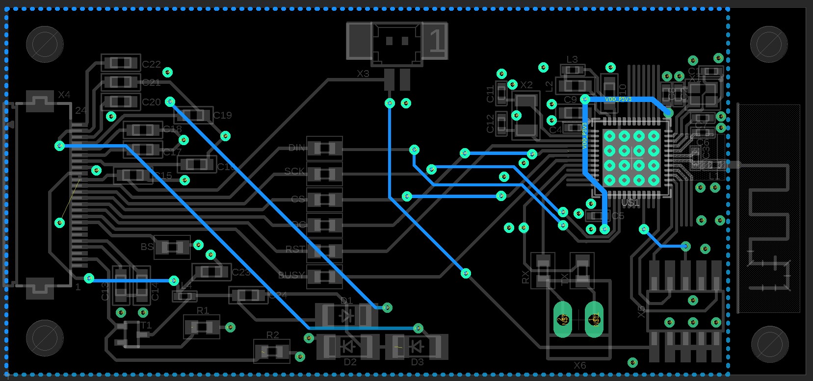
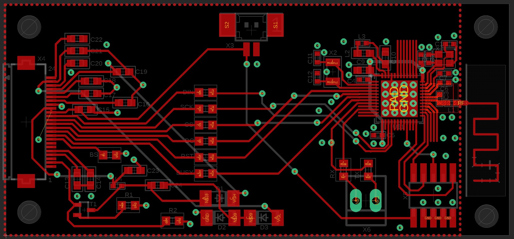
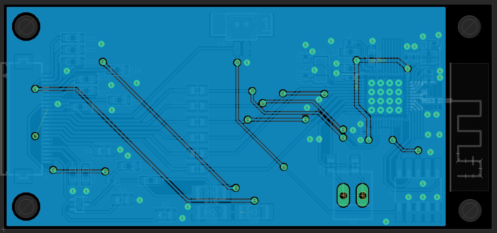
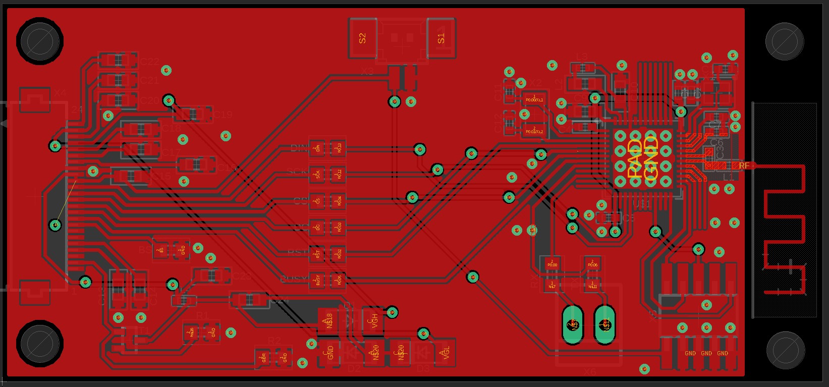
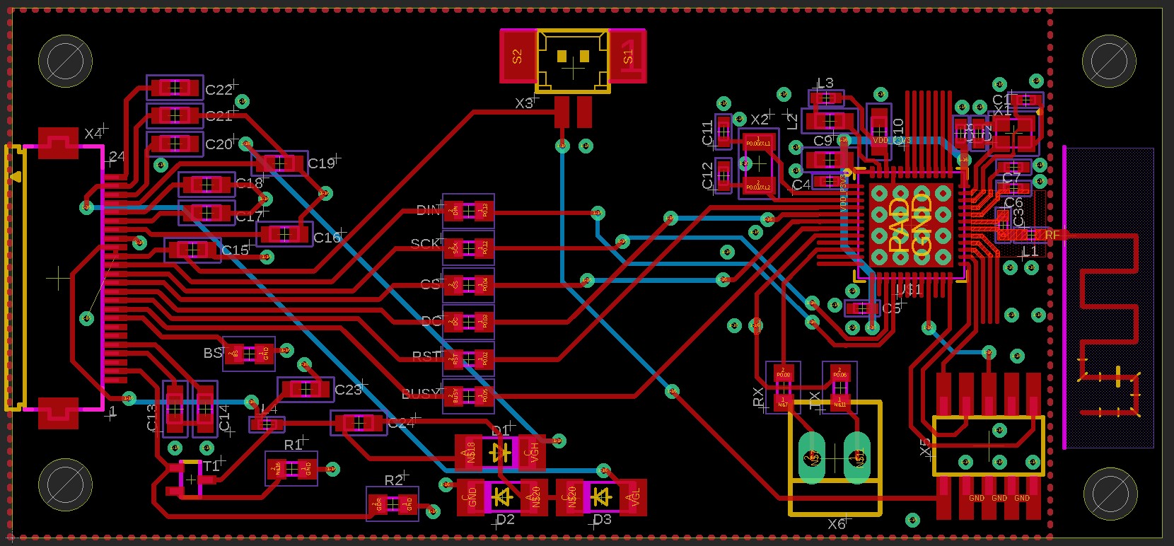
I have made this PCB design with the help of a reference circuit to run an e-paper display with an nRF52810.

I have doubts about the followings:

  1. Do signal track lengths or widths need to change?
  2. Is there a track path that I am supposed to avoid?
  3. Do I have to reposition any of the components, such as the capacitor?
  4. Is the antenna position good for 2.45 GHz?
  5. Anything else that I can do to make the design better?

PCB images:

enter image description here

Note: The reason I added 0 Ω resistors to the DIN, SCK, CS, DC, RST, and BUSY signal lines is to get a point to check the signal on these lines; similar reason for RX & TX line 0 Ω resitors.

enter image description here

enter image description here

With copper pour: enter image description here

enter image description here

PCB: Board/schematic Eagle file and schematic PDF files here

Below some circuit references:

  1. nRF52810 Minimal Circuit (Reference here).

  2. EPD driver circuit reference is here

Please ignore the via under the 24-pin FPC connector on the left side which has a trace to the VCC pin. I don't know why it was showing in the first place, but I corrected it now with its connection to GND.

Reference nRF52810 QFAA DCDC, here

\$\endgroup\$
16
  • \$\begingroup\$ ah okay, so improve? \$\endgroup\$ Commented Oct 22, 2022 at 10:00
  • 1
    \$\begingroup\$ Instead of adding 0 ohm resistors (each with 2 pads and a component placement) to create a test point why not just add a small SMD SIP header along the group of traces? You wouldn't need to install the header component and you would have a single open pad for a test point. (There may actually be single pin test point components in your available component library.) \$\endgroup\$
    – Nedd
    Commented Oct 22, 2022 at 10:29
  • 1
    \$\begingroup\$ It might be helpful to slide the X5 and X6 connections further away from the antenna traces, The chip mfg might have recommended clearances for placing other components near the antenna traces. As for the antenna itself, be sure to follow the mfgr's details for shape, layering, and size as accurately as possible. \$\endgroup\$
    – Nedd
    Commented Oct 22, 2022 at 10:50
  • 1
    \$\begingroup\$ @JustdoinGodswork Do you want only PCB design advice? Or also schematic design advice? Or circuit design advice? Because not all things are only about designing the PCB. \$\endgroup\$
    – Justme
    Commented Oct 22, 2022 at 11:05
  • 1
    \$\begingroup\$ You are breaking up your bottom ground pour with long traces, effectively weaken it a lot. If your switch/strobe/clock frequency is low enough and everything have strong local decoupling, you can probably get away with it. If not, try to avoid long traces on that layer by routing most of it on top layer and only use short tracks on bottom when you need to cross something on top layer. “Stitching” the track via top and bottom, while avoiding bottom. Even better, try to do floorplanning of parts, where and on which sides to avoid long tracks all together. How does your decoupling situation look? \$\endgroup\$
    – winny
    Commented Oct 22, 2022 at 11:42

2 Answers 2

2
\$\begingroup\$

If you haven't made too many changes already here is another group of improvements to consider.

Improve the long trace coming from X4 p23:
Move C22 up slightly, catch the X4 P23 connection at the left pad of C21 then route to the right and down, cross the horizontal group of traces at a minimum length location. Continue routing to D3 but now go above D1. Rearrange again after other changes.

Tighten up traces at the center of the board and minimize vertical bottom trace lengths:
The 0 ohm resistors can be staggered horizontally then their traces brought closer together.
Move DIN resistor left about 1/2 the length of the resistor.
Move SCK resistor right just beyond the edge of the DIN resistor, then move resistor up tight against DIN trace.
Move CS resistor left beyond SCK resistor, then move up tight against SCK trace.
Repeat with DC, RST, and BUSY resistors.
The extra space below the resistors should now allow more space to route D1, D2, D3 traces.
The reduced width of all these traces will now minimize the trace length needed to cross the board.
Reroute D1 long diagonal trace (on top side first), then continue under the BUSY resistor then left, place via to jump over the minimum length point of the horizontal trace group, add another via and route to C19.

Reduce the center vertical trace lengths on bottom side:
Slide the RST long diagonal trace right, then slide DC long diagonal trace (and via) right, then slide the BUSY long diagonal trace left (with an extra angle segment), reroute long X3 trace (on top side first) down to the DC trace then place a via, cross DC, DST and BUSY, place via, route to X5.

To clean up the lower left of the board:
Rotate C14 ccw, move upward.
Rotate C13 ccw, move upward close to C14.
Move R2 under C13, connect directly to X4 p2.
Move T1 right.
Rotate R1 180 deg, move to left side of T1.
Move R1 and T1 further away from mounting hole.
Move L4 to left of T1 and above R1, connect to T1 under body.
Move C24 down in line with D2.
Move C23 to left of T1.
Slide D1, D2, and D3 left to minimize trace lengths.

Improve X6 area:
Move TX resistor to left of RX resistor, route TX trace to bottom of X6 p1 pad.
Move both RX and TX resistors upward so that they are clear of the corner of X6.

Improve gnd connections at top left:
Give C19 its own gnd via to right of pad.
Give C16 its own gnd via to right of pad (move other trace if needed).
Give C21 its own gnd via to right of pad.
Move C15 gnd via closer to C15 pad.
Reroute long trace from C19 (on top side first) to minimize required bottom trace length.

Improve X4 pin to pin connection (if this is not an error):
Remove the tiny existing trace within the tight finger area.
Slide C15 slightly to the right.
Move the via on X4 p17 to the right.
Make the X4 p16-15 connection outside the finger area.

Extra via under X4:
If this extra via was previously connected to a pin it may still have the net name associated with it. As long as the original net is now fully routed just delete the via.

\$\endgroup\$
3
\$\begingroup\$

Just some observations:

If EMC is a concern, I would strongly recommend using four layers with at least one solid reference plane (recessed under the antenna). Or, if you want/need to stick to two layers, at least keep signal lengths on the bottom layer to an absolute minimum to have a as solid as feasible reference plane.

The board isn't 100% routed. The line under the big connector on the left appears to be an air wire.

The thermal vias under the chip on the right will suck away solder. However, that might not be much of a problem for a hand-soldered prototype.

If neighboring pins of chips or connectors are on the same net, I would avoid connecting them with an as short as possible track as that might end up looking like an unintentional short after soldering. It might be okay with the chip on the bottom right as there should be enough solder mask between the pins. The connector on the left appears to be a finer pitch, so here I would consider avoiding a direct connection. That depends on the solder mask capabilities of your PCB fab, of course.

\$\endgroup\$
3
  • \$\begingroup\$ as winny mentioned also, i'll definetly going to improve the bottom layer to minimal signal tracks. Left unrouted tacks I mentioned in the edited, idk why it cam but I fixed it to ground now. What can I do else for left connector (24 pin FPC connector), shall I use via with those pns? if avoiding direct connection? \$\endgroup\$ Commented Oct 22, 2022 at 16:53
  • \$\begingroup\$ @JustdoinGodswork In this case it should be possible to add a track to the left of the lower pad and connect it with the trace that is leaving the upper pad. Just avoid copper between the pads. It might be totally fine the way it is, depending on the circumstances (PCB fab capabilities, soldering technique, ...). But it's a good idea to avoid those direct connections when practicable. \$\endgroup\$
    – feynman
    Commented Oct 22, 2022 at 17:23
  • \$\begingroup\$ Re air wires: "You may know those two nodes are on the same net, and I may know they're on the same net, but are the electrons going to know that?" \$\endgroup\$
    – supercat
    Commented Oct 22, 2022 at 17:51

Your Answer

By clicking “Post Your Answer”, you agree to our terms of service and acknowledge you have read our privacy policy.

Not the answer you're looking for? Browse other questions tagged or ask your own question.