I am trying to add a 20MHz external crystal oscillator to my PIC18F4550 microcontroller. The external crystal oscillator circuit connections to the PIC18F4450 is as below:
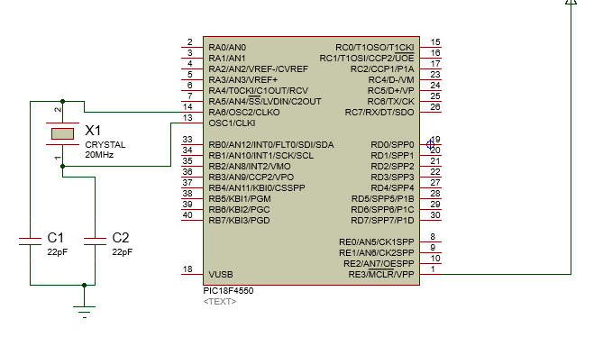
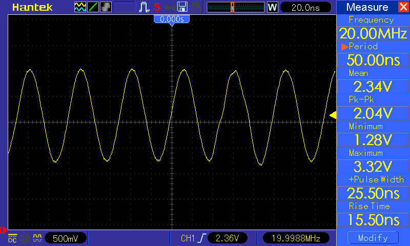
The Datasheet suggest to use 15pF capacitors for 20MHz crystal however, I have used 22pF by mistake. With that said, when I try to hook up my oscilloscope to check the PIN13 (OSC1) of PIC18 microcontroller, I am able to see the 20MHz sine wave signal present as below. So I decided against replacing the existing 22pF capacitors with 15pF capacitors.
Then, I used the following code to create a shortest pulse width possible at LATB7.
// PIC18F4550 Configuration Bit Settings

// 'C' source line config statements

// CONFIG1L
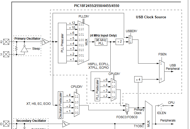
#pragma config PLLDIV = 5       // PLL Prescaler Selection bits (No prescale (4 MHz oscillator input drives PLL directly))
#pragma config CPUDIV = OSC1_PLL2// System Clock Postscaler Selection bits ([Primary Oscillator Src: /1][96 MHz PLL Src: /2])
#pragma config USBDIV = 1       // USB Clock Selection bit (used in Full-Speed USB mode only; UCFG:FSEN = 1) (USB clock source comes directly from the primary oscillator block with no postscale)

// CONFIG1H
#pragma config FOSC = HS // Oscillator Selection bits (Internal oscillator, HS oscillator used by USB (INTHS))
#pragma config FCMEN = OFF      // Fail-Safe Clock Monitor Enable bit (Fail-Safe Clock Monitor disabled)
#pragma config IESO = OFF       // Internal/External Oscillator Switchover bit (Oscillator Switchover mode disabled)

// CONFIG2L
#pragma config PWRT = OFF       // Power-up Timer Enable bit (PWRT disabled)
#pragma config BOR = ON         // Brown-out Reset Enable bits (Brown-out Reset enabled in hardware only (SBOREN is disabled))
#pragma config BORV = 3         // Brown-out Reset Voltage bits (Minimum setting 2.05V)
#pragma config VREGEN = OFF     // USB Voltage Regulator Enable bit (USB voltage regulator disabled)

// CONFIG2H
#pragma config WDT = OFF         // Watchdog Timer Enable bit (WDT enabled)
#pragma config WDTPS = 32768    // Watchdog Timer Postscale Select bits (1:32768)

// CONFIG3H
#pragma config CCP2MX = ON      // CCP2 MUX bit (CCP2 input/output is multiplexed with RC1)
#pragma config PBADEN = ON      // PORTB A/D Enable bit (PORTB<4:0> pins are configured as analog input channels on Reset)
#pragma config LPT1OSC = OFF    // Low-Power Timer 1 Oscillator Enable bit (Timer1 configured for higher power operation)
#pragma config MCLRE = ON       // MCLR Pin Enable bit (MCLR pin enabled; RE3 input pin disabled)

// CONFIG4L
#pragma config STVREN = ON      // Stack Full/Underflow Reset Enable bit (Stack full/underflow will cause Reset)
#pragma config LVP = OFF         // Single-Supply ICSP Enable bit (Single-Supply ICSP enabled)
#pragma config ICPRT = OFF      // Dedicated In-Circuit Debug/Programming Port (ICPORT) Enable bit (ICPORT disabled)
#pragma config XINST = OFF      // Extended Instruction Set Enable bit (Instruction set extension and Indexed Addressing mode disabled (Legacy mode))

// CONFIG5L
#pragma config CP0 = OFF        // Code Protection bit (Block 0 (000800-001FFFh) is not code-protected)
#pragma config CP1 = OFF        // Code Protection bit (Block 1 (002000-003FFFh) is not code-protected)
#pragma config CP2 = OFF        // Code Protection bit (Block 2 (004000-005FFFh) is not code-protected)
#pragma config CP3 = OFF        // Code Protection bit (Block 3 (006000-007FFFh) is not code-protected)

// CONFIG5H
#pragma config CPB = OFF        // Boot Block Code Protection bit (Boot block (000000-0007FFh) is not code-protected)
#pragma config CPD = OFF        // Data EEPROM Code Protection bit (Data EEPROM is not code-protected)

// CONFIG6L
#pragma config WRT0 = OFF       // Write Protection bit (Block 0 (000800-001FFFh) is not write-protected)
#pragma config WRT1 = OFF       // Write Protection bit (Block 1 (002000-003FFFh) is not write-protected)
#pragma config WRT2 = OFF       // Write Protection bit (Block 2 (004000-005FFFh) is not write-protected)
#pragma config WRT3 = OFF       // Write Protection bit (Block 3 (006000-007FFFh) is not write-protected)

// CONFIG6H
#pragma config WRTC = OFF       // Configuration Register Write Protection bit (Configuration registers (300000-3000FFh) are not write-protected)
#pragma config WRTB = OFF       // Boot Block Write Protection bit (Boot block (000000-0007FFh) is not write-protected)
#pragma config WRTD = OFF       // Data EEPROM Write Protection bit (Data EEPROM is not write-protected)

// CONFIG7L
#pragma config EBTR0 = OFF      // Table Read Protection bit (Block 0 (000800-001FFFh) is not protected from table reads executed in other blocks)
#pragma config EBTR1 = OFF      // Table Read Protection bit (Block 1 (002000-003FFFh) is not protected from table reads executed in other blocks)
#pragma config EBTR2 = OFF      // Table Read Protection bit (Block 2 (004000-005FFFh) is not protected from table reads executed in other blocks)
#pragma config EBTR3 = OFF      // Table Read Protection bit (Block 3 (006000-007FFFh) is not protected from table reads executed in other blocks)

// CONFIG7H
#pragma config EBTRB = OFF      // Boot Block Table Read Protection bit (Boot block (000000-0007FFh) is not protected from table reads executed in other blocks)

// #pragma config statements should precede project file includes.
// Use project enums instead of #define for ON and OFF.

#include <xc.h>
#include <pic18f4550.h>

#define _XTAL_FREQ 20000000
#define LED LATBbits.LATB7
#define ON 1
#define OFF 0

void main(void) {
    TRISBbits.TRISB7 = 0;
    while(1)
     {
        LED = ON;
        NOP();
        LED = OFF;
     }
     }
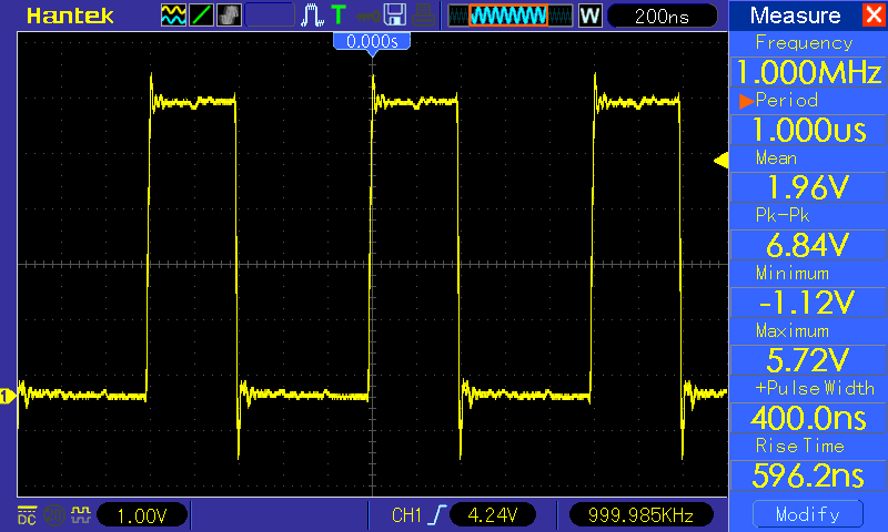
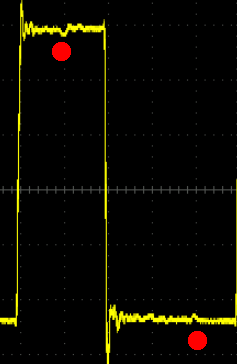
However, when I monitor the output pin RB7 with oscilloscope, it appears the the pulse width is around 400ns.
Since the frequency is 20MHz, each cycle would be 50ns. Assuming PIC18F4550 need 4 clock cycles for 1 instruction cycle, shouldn't I be able to achieve a lower pulse width than 400ns? What am I missing?
EDIT 1: Assembly listing of the main loop:
78:            void main(void) {
79:                TRISBbits.TRISB7 = 0;
7FF0  9E93     BCF TRISB, 7, ACCESS
80:                while(1)
81:                 {
82:                    LED = ON;
7FF2  8E8A     BSF LATB, 7, ACCESS
83:                    NOP();
7FF4  F000     NOP
84:                    LED = OFF;
7FF6  9E8A     BCF LATB, 7, ACCESS
7FF8  EFF9     GOTO 0x7FF2
7FFA  F03F     NOP
7FFC  EF00     GOTO 0x0
85:                 }
86:                 }
EDIT 2: As Tom Carpenter Suggested, I have changed my CONFIG1L and CONFIG1H as follow:
// CONFIG1L
#pragma config PLLDIV = 5       // PLL Prescaler Selection bits (No prescale (4 MHz oscillator input drives PLL directly))
#pragma config CPUDIV = OSC1_PLL2// System Clock Postscaler Selection bits ([Primary Oscillator Src: /1][96 MHz PLL Src: /2])
#pragma config USBDIV = 1       // USB Clock Selection bit (used in Full-Speed USB mode only; UCFG:FSEN = 1) (USB clock source comes directly from the primary oscillator block with no postscale)

// CONFIG1H
#pragma config FOSC = HSPLL_HS // Oscillator Selection bits (Internal oscillator, HS oscillator used by USB (INTHS))
#pragma config FCMEN = OFF      // Fail-Safe Clock Monitor Enable bit (Fail-Safe Clock Monitor disabled)
#pragma config IESO = OFF
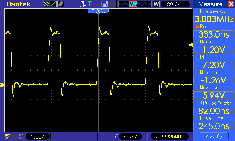
As the CPU clock is now 48MHz, each cycle takes 20.83ns. One instruction cycle is 83.33ns. My oscilloscope result match the expectation (Although the output waveform is much distorted at this point - perhaps a separate topic to discuss). Thank you all for your comprehensive answers.


main()loop? Or disassemble it from the object file? \$\endgroup\$