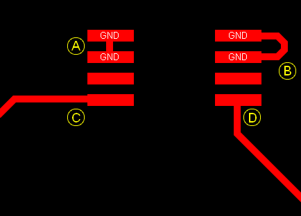
(C) vs. (D):
I don't think there are any significant advantages to one or the other.
(A) vs. (B):
I would default to (B). The reason is that (A) can look like an unintentional short after soldering. Especially with finer pitch devices there might be not enough solder mask between the pads to prevent the solder from flowing over the little trace to the other pin to form one big chunk of solder. Or the PCB manufacturer may have removed the solder mask between the pads altogether due to their solder mask capabilities.
It might look something like this:

You can't see it on the picture, but the five most left pins have that exact (A) connection with short traces between the pads. It's not a real problem, of course. But it might cause unnecessary concern to someone or something (AOI) inspecting the board. One might even argue that those solder joints could be weakened, because there is a lot of solder in places where it's not supposed to be (on and/or between the pins instead of forming nice fillets at the heel and the toe of the pin).
Sometimes you don't have the space for (B), of course. And wider pitch packages like SOIC shouldn't be as prone to this phenomenon.
But like I said: I would default to (B).


