2
\$\begingroup\$

I have built three very high input impedance amplifiers; under 1 pF, over 100 MΩ.


One some else's design and layout, very high input impedance, but low frequency; several MHz. Not shown below.


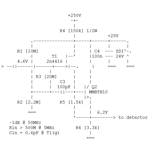
The second one I layed out hoping frequency response to 30 MHz, but it dropped off of 17 MHz. Probably poor layout.

mix of SMD and through hole pcb

enter image description here


For the next one I received advice to skip the SMD and use through-hole (seems counter intuitive).

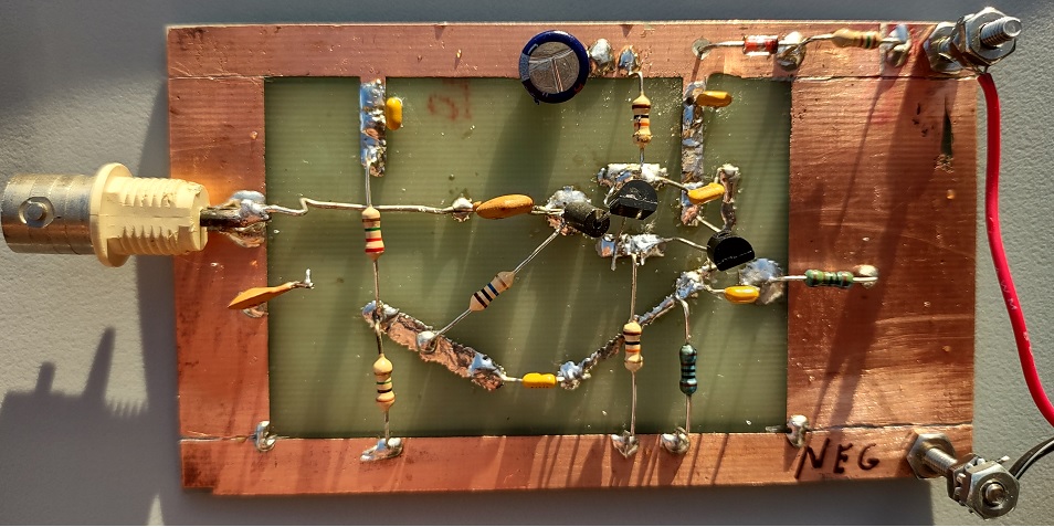
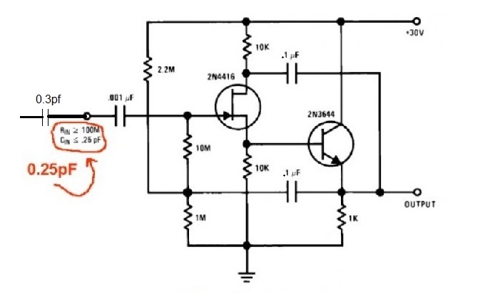
It is a different schematic and is supposed to reach 90 MHz, it did pretty well, but had a level bump at 29 MHz, I had etched away the underside ground plane, I covered it with a grounded copper tape and that removed the level bump and it is pretty flat to 30 MHz, well under 1 dB.

pictures of my first and second lay out.

Note: I did have the 0.3pf cap on the input of both


Now I want smaller, so I'm going through the learning curve of learning KiCad to design an SMD high input impedance PCB.

Any hints on how to limit the strays that cause problems?

\$\endgroup\$
5
  • \$\begingroup\$ Welcome! A really high impedance board is an empty board. Which is to say: This question is pointless without specs and schematics. \$\endgroup\$
    – tobalt
    Commented Nov 22, 2022 at 18:37
  • \$\begingroup\$ Yes, the first one is low frequency and I didn't post it. The second one is the Dremeled pcb with and ascii art schematic, The third, thru hole resistor board is a regular schematic and is labeled 0.25pf 100MΩ input. \$\endgroup\$ Commented Nov 22, 2022 at 21:06
  • 1
    \$\begingroup\$ @MikeKnowlton - Thanks. I have moved the schematics so they are next to the photo of the relevant board as you described, to help readers. || Personally, I'm concerned that this photo does not match the "regular schematic" e.g. (a) large electrolytic cap in photo (top centre) not shown in schematic; (b) diode in photo (top right) not shown in schematic. But since you have said that this is the schematic for that board, I must be somehow misinterpreting the photo. \$\endgroup\$
    – SamGibson
    Commented Nov 22, 2022 at 21:24
  • 1
    \$\begingroup\$ @MikeKnowlton - Please edit your question to add the source links for any material which isn't your original work (e.g. the schematics), as required by this site rule (or best efforts for offline sources - see that rule). FYI someone created the 2nd schematic in your question by slightly altering the schematic from old National Semiconductor AN-32 FET Circuit Applications (reissued by TI). Since you're new here, please view the tour & help center to see how SE differs from typical forums \$\endgroup\$
    – SamGibson
    Commented Nov 22, 2022 at 22:38
  • \$\begingroup\$ Hi all, yes that is the schematic from AN32, I copied into my pictures over 10 years ago, I knew it was from a data book, but not which one, recently I decided to build it. I added a 0.3pf to the input to lower the input capacitance. My supply is about about 37V, so I added a dropping resistor, zener and filter cap, I placed a couple of bypass caps on the circuit. The only person that gave any tips about laying out pcbs for high impedance circuits is Spehro. Feel free to delete the thread, I tried but was not allowed. \$\endgroup\$ Commented Nov 23, 2022 at 22:25

1 Answer 1

2
\$\begingroup\$

Maybe you can play with the circuit in simulation with various parasitic capacitances added. The effects are reduced by maybe 5:1 (but not eliminated) by the bootstrapping.

You could consider using a string of resistors for the gate bias resistor, for example.

Extending bootstrapped copper under (or around but not under) the resistor body and input conductor may also be effective. That connector must contribute significantly.

Using through-hole components for the JFET and input bias resistor may be helpful because you can get them off the PCB (with its high K \$\approx\$ 4) and into the air (with K = 1).

At 30MHz, 1pF of capacitance has impedance of around 5kΩ, so the impedances are not really particularly low, rather the effective input capacitance is low.

\$\endgroup\$
2
  • \$\begingroup\$ On the connector, that was only there until I got it working, then I removed it and add a 0.3pf on the input. \$\endgroup\$ Commented Nov 22, 2022 at 23:27
  • \$\begingroup\$ On the connector, that was only there until I got it working, then I removed it and add a 0.3pf on the input. I think I have been lumping high frequency pcb design with high impedance design, I thought smd was the way to build a high input impedance, keeping things small, but then was told to go to thru hole, and that worked. \$\endgroup\$ Commented Nov 23, 2022 at 3:28

Your Answer

By clicking “Post Your Answer”, you agree to our terms of service and acknowledge you have read our privacy policy.

Not the answer you're looking for? Browse other questions tagged or ask your own question.