1
\$\begingroup\$

I relatively new to working with MCU's and have been having some trouble figuring out what "mode" to set a pin to when trying to map it to the correct function. For this project, I am using a STM32L431VCT6 and I am just trying to wrap my head around what mode to set the pin to to correctly fit with what the schematic of this device is showing.

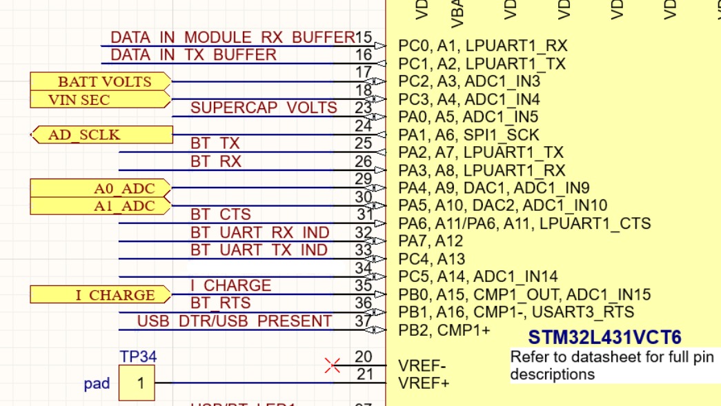
Portion of the schematic: STM Schematic

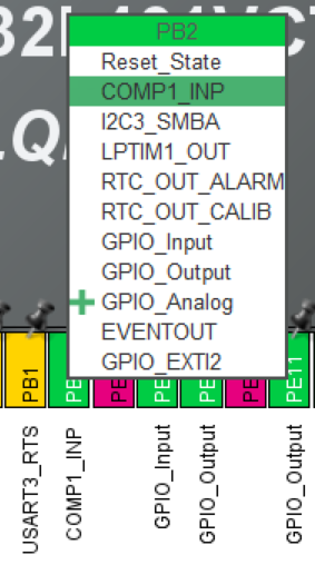
So from what I understand, the red is the input/output signal to/from that pin, and the black writing on the micro are the modes the pin is capable of. Now if I go to my STM32CubeMX application, and select pin 37 which is USB DTR/USB PRESENT on the schematic, I am presented with a series of options. How can I figure out what one to choose? I've selected COMP1_INP for the pin 37, but could it also be GPIO_Input?

STM Cube Pin Layout: STM Cube Pin Layout

I've had a look at the data sheet for that pin, and it doesn't seem to give me much info other than its alternative modes.

Any help or pointers would be really appreciated.

\$\endgroup\$
3
  • \$\begingroup\$ The alternative modes are what matters though. Names like PA1, PB2, or PC5 is the actual name of they physical pin and tells you which GPIO port (letter) it is on. But beyond that what the pin is actually doing is probably dictated the alternative function it is set to. \$\endgroup\$
    – DKNguyen
    Commented Dec 5, 2022 at 4:57
  • \$\begingroup\$ Those are alternate functions for the pin. Pin modes would be input, output, GPIO or alternate. For PB2, you would use it as compatator inout only if you know that the signal must be read through the analog comparator. If it is a logic level signal, why use the comparator. \$\endgroup\$
    – Justme
    Commented Dec 5, 2022 at 5:47
  • 1
    \$\begingroup\$ The red writing is the net name assigned to the net by the person who designed the circuit. Your job as the firmware engineer is to pick the most appropriate pin mode for the mcu pin connected to that net. To me, something like USB DTR/USB PRESENT seems like it should be a simple GPIO Input or possibly an edge triggered interrupt. COMP1_INP would be the input to an analog comparator, which didn't seem like a useful choice for something labeled USB DTR/USB PRESENT. \$\endgroup\$
    – brhans
    Commented Dec 5, 2022 at 5:50

1 Answer 1

1
\$\begingroup\$

The hardware designer should be giving you (a lot) more information. At least something like a block diagram, and a description of how each pin should interact with the external hardware.

As a hint, this chip does not have a USB interface. Also, DTR (Data Train Ready) is an acronym associated with a serial interface such as RS-232.

So I might guess that you'll find a USB-serial chip such an FTDI or CH340 part somewhere on the board, with TxD and RxD connected to one of the three available on-chip UARTs, and that the chip has a DTR output. Since it's not part of the standard driver 'hardware handshaking' (RTS & CTS are) it's probably just in need of a regular GPIO pin configured as input. Whether it needs to be configured as a pullup, pulldown or neither should be determined.

\$\endgroup\$

Your Answer

By clicking “Post Your Answer”, you agree to our terms of service and acknowledge you have read our privacy policy.

Not the answer you're looking for? Browse other questions tagged or ask your own question.