1
\$\begingroup\$

The problem is on a circuit which implements PFC circuitry.

There are two parallel 0.36R current sense resistors located in the inrush current path. These resistors measure the PFC current through the ground return path. They are exposed to the inrush currents and these inrush current amplitudes tend to change according to the impedance of the AC grid and the initial angle under which the AC grid has started to operate. It has been observed that these current sense resistors become open-circuit after they are exposed to the inrush current.

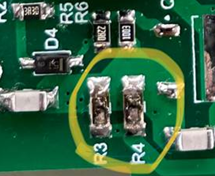
The resistors are 1206 package SMD resistors and I have attached their locations on the PCB below. It has been observed that the inrush current is larger under the condition that the circuit is energized directly from the AC grid. The breakdown happened just as we plugged in the device to the line.

In my opinion, the IC has been damaged because the inrush current could've passed through the respective pin on the IC. The impedance of the line is varying region by region in our country. The resistor should be selected in such a way that it should handle the worst case scenario, which is the minimum line impedance.

We have also realized that pad to pad clearance of these resistors may be closer than the isolation requirements. I'm just wondering if the applied voltage breaks down the isolation between the pads. Could it be possible that this outcome may have occured after this effect?

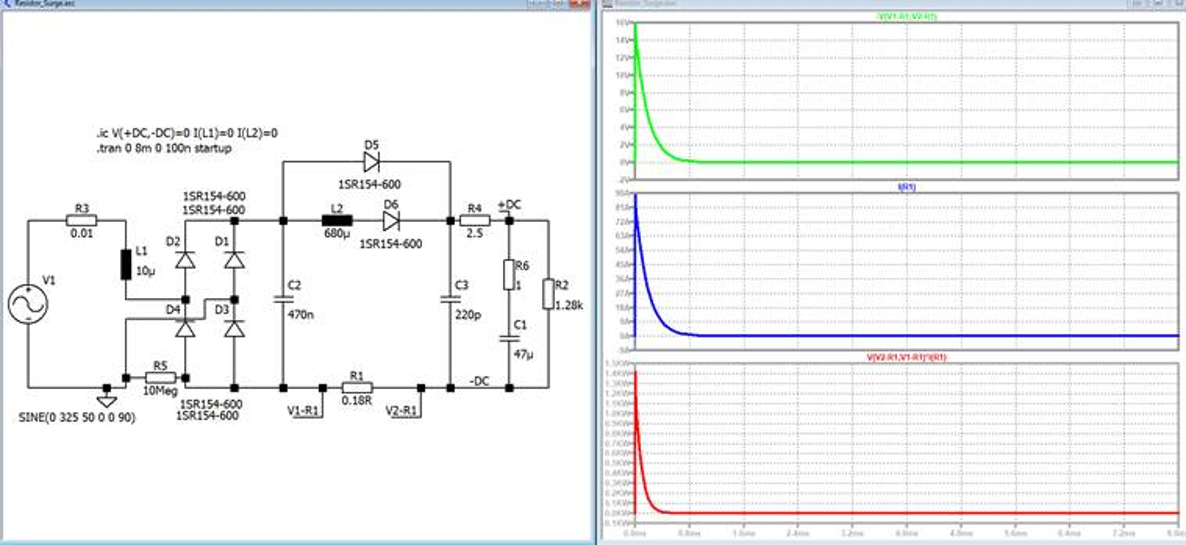
Below in the simulation screenshots (notice that 0.18R represents 2x0.36R parallel resistors), it can be seen that the insantaneous power losses caused by the inrush current go up to the 1 kW level. I would be very glad if you could tell me what could be the root cause for this problem. The inrush current is the best explanation I can bring to this problem but I would like to hear your contributions on this matter as well. Also I would be very glad if you could help me with resistor selection under such parameters. Because I cannot find the single pulse curves in some datasheets.

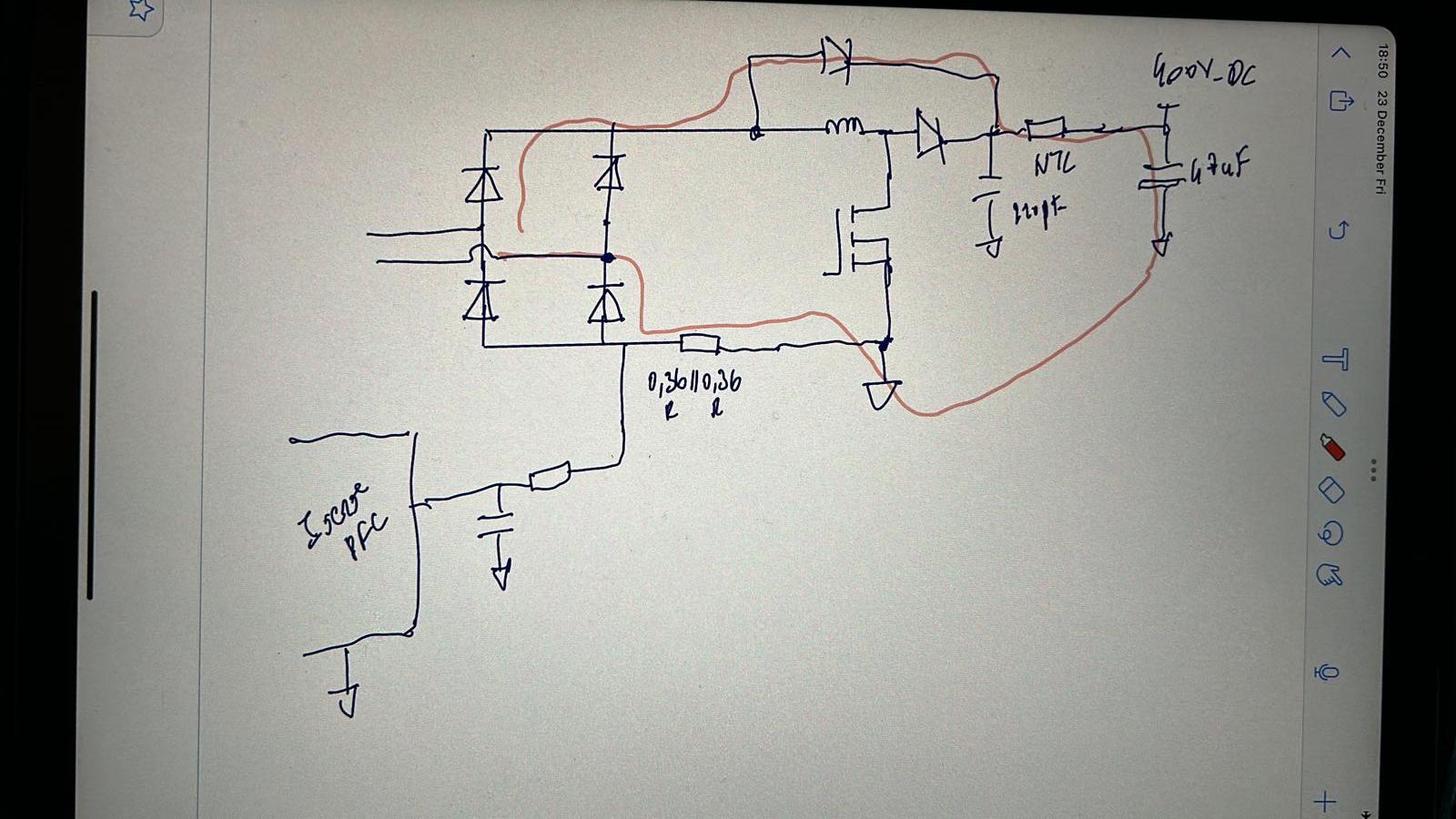
Schematic

PCB layout of the specific area

Simulation results

\$\endgroup\$
16
  • \$\begingroup\$ Why not use a single 2512 etc instead? \$\endgroup\$
    – Lundin
    Commented Jan 3, 2023 at 11:06
  • 2
    \$\begingroup\$ Could you please post a schematic which is actually matching the PCB layout? They don't seem to have a lot in common... \$\endgroup\$
    – Lundin
    Commented Jan 3, 2023 at 11:09
  • \$\begingroup\$ I'd like to understand the root cause of the problem first. If the problem is what I think, then I will consider making a revision the PCB layout. The schematic on the simulation is just to characterize the high inrush current behaviour. \$\endgroup\$
    – ohkann_
    Commented Jan 3, 2023 at 11:23
  • 1
    \$\begingroup\$ Well to begin with, why is there a 100k resistor instead of a 10M one? It should be saying 10005. \$\endgroup\$
    – Lundin
    Commented Jan 3, 2023 at 11:29
  • 2
    \$\begingroup\$ "I cannot share neither the PCB layout nor the schematic completely because of the data privacy." Too bad. Because I was really looking for an opportunity to steal a non-working design... \$\endgroup\$
    – Lundin
    Commented Jan 3, 2023 at 13:05

2 Answers 2

1
\$\begingroup\$

When charging a capacitor through a resistance, the energy absorbed in the resistance is equal to the energy transferred to the capacitor. The resistors in the charging circuit need to be able to absorb and dissipate this amount of energy. Charging power is a function of the initial phase. In the worst case, near the line voltage peak, the charging time is shortest, around 3 RC (time constants), and average power is max. But the total energy is not a function of the line voltage initial phase, and line impedance can be neglected. Total energy determines how hot the resistors become, since charging times are short.

Your circuit sketch shows an NTC between the diode and the capacitor. Its characteristics are not mentioned, but it is in the charging path. An NTC is one way to deal with inrush current. When using an NTC, it must be sized carefully. It can be tricky to get the right balance: if too small it will be overstressed by the inrush current, leading to failure; too large it won't warm up enough to drop its resistance. Also, NTCs can be less effective if power is cycled off and back on before the NTC can cool down. (By the way, I'm not used to seeing an NTC in that position. More typically they are in the line before the rectifier bridge.)

Your current sense resistors also need to be able to handle the inrush; they need to be big enough to absorb their share of the energy without damage. Given the lack of specifics, it's hard to say for sure, but it seems like a couple of 1206s might be rather undersize

There is another way to handle inrush, a bit more complicated (and costly). That is to provide a soft start circuit - a separate charging circuit that is bypassed, typically with a MOSFET, once the capacitor is charged. With this method the charging time can be increased, reducing peak power dissipation in the charging components.

\$\endgroup\$
0
\$\begingroup\$

I would be very glad if you could tell me what could be the root cause for this problem.

The resistors are physically too small. They can't handle the heat. Have you played with axial resistors and a bench power supply? The bigger ones can handle the same power for much longer, or a higher power for the same time as the small ones before they go up in smoke.

help me with resistor selection under such parameters

Use physically larger resistors. Resistor peak power handling scales with an exponent between the square and cube of linear dimensions.

The resistors must also have a rated maximum operating voltage across terminals that's well in excess of nominal line conditions. Say 500-600V at least. That'll help establish the minimum size for each resistor product series (manufacturer's series).

I cannot find the single pulse curves in some datasheets

That's a way of the manufacturer telling you "if you want to do peak loading beyond continuous power rating, you're on your own". Interpretation: buy different resistors that have this rating, or experimentally qualify un-rated products for your application. That's potentially a lot of work.


If you do this sort of design work, you should have hopefully reverse engineered several random supplies on the market just to see if there's anything there to learn. It's either that or a design review process with experienced mentors who know all this already, or can figure it out quickly. I mean, you need to learn this stuff from somewhere, so if you want to save time on self-learning while doing product design, you have to reverse-engineer and make sure you can follow the decisions made by some other team.

\$\endgroup\$

Your Answer

By clicking “Post Your Answer”, you agree to our terms of service and acknowledge you have read our privacy policy.