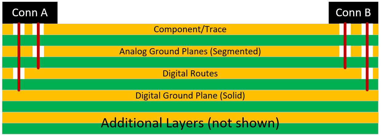
You have "digital routes" coupled to (i.e. sandwiched between) "analog" and "digital", which is to say, it's stripline. The vendor has spotted this correctly.
As a thought experiment, consider: if you wanted L3 to couple only to L4, how would you do it? Surely the environment is symmetrical with respect to the trace -- locally speaking, it doesn't know which is which, it's just a strip of metal between two other sheets of metal. The only thing you can do is increase height from one plane (i.e. use very thick prepreg L2-L3 and thin L3-L4). The other thing is to shield it completely, adding another digital ground layer (could also be VCC or whatever, DC voltage doesn't matter) before the analog plane.
I think your thought process might be making the assumption that, since the analog plane isn't grounded on the far end, there's nowhere for those induced currents to flow out (near Conn B). But this is not the case: image currents (in general: coupling between adjacent bits of metal) are a local phenomenon, and a loop will be found somehow or another. Leaving the plane open on one side, just means all that coupled energy raises the voltage of the plane on that side. Which eventually finds its way back into the single-point grounding via/pad, and back and forth, a standing wave system, hence ringing waveforms will be found (if excited by suitable harmonics, that is).
We can simplify this model as a transmission line on one plane, with a small transformer element coupling into the LC resonant tank formed by the poorly-grounded plane's inductance and capacitance. This does several things: it disturbs the ground voltage (analog with respect to digital, particularly at points far away from Conn A), it worsens signal quality (the ringing waveform couples out of / back into the digital traces), and probably most important is it breaks the assumption that analog ground is quiet (with respect to other parts of the PCB, anyway).
A more detailed model might consider the wave behavior of the plane(s), since the "segmented" shapes are probably weird, and waves propagate within its 2D space, reflecting off the boundary (open circuits) and stitching vias (short circuits). These effects may be at high enough frequencies (i.e. a few ~cm wide pour has resonances in the low to fractional GHz) that you aren't concerned about them (say the digital signals are LVCMOS, 2~5ns risetime, harmonics out to mid 100s MHz). Perhaps it's a problem when the digital signals are higher bandwidth (SDRAM would be the biggest concern I think; most other high speed comms these days are differential), or the planes are bigger (10s cm?), or the analog is more sensitive (~µV, and wideband or RF?).
Trying to separate grounds is generally a foolish errand; you easily encounter traps like this, and it's harder and harder to reason about which components and signals are running with respect to which reference planes.
It's much easier to separate currents: route the digital signals away off one side of Conn A. If possible, place Conn B adjacent to Conn A to close the loop (of the digital currents) not just off to one side but with short length as well, meaning there's nowhere for the currents to spread out into. Use same GND through the board stack and stitch them together religiously. The analog section will be quiet simply because there's no currents flowing across it. Supplies and lower bandwidth signals can be brought into the area with local filtering (ferrite beads, RCs, etc.) to further isolate the region.
Currents can be further separated by cutting slots through the entire board, but this must be done even more carefully than multiple reference planes, I would say. The problem is, currents want to flow along the shortest path (namely, paths of least inductance), and putting a slot in the middle of such a path, forces currents right to the edge of that slot. The slot can emit EMI, or indeed induce current across its width so that you've not actually accomplished much by making it. (The size of this magnetic field is comparable to the layer spacing, so make the slot at least several layer spacings wide. So, for a typical PCB build, ~1mm minimum.) And needless to say, the slot must not be crossed by signal traces lest it act as a slot antenna, coupling harmonics from the signals into free space (and vice versa).
Basically, use the signals' own preference (paths of least impedance) to solve the grounding for you.
Unfortunately I can't suggest an alternative without knowing more about the system. To be clear, EMC is a holistic study; it requires knowledge of the whole system, not just what's on a given board, but what the board connects to, and the environment those board(s) and connections are exposed to. There is no detail too small to omit.

