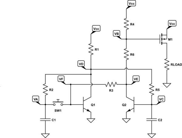
This circuit was found on various electronic web sites
Sometimes that's a problem: the circuit might not have been tested, or might have been a starting point for further exploration. It's not a given it's supposed to work at all.
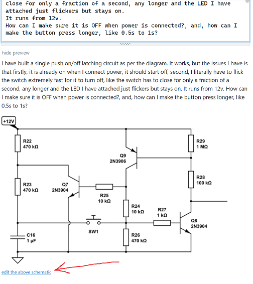
The LED is connected to the collector of Q8 via a 2n3906 transistor.
Please edit the schematic to add that transistor, by clicking "Edit" on the question, then "Edit this schematic" under the schematic in the preview below the edit window:

This answer will be updated once you present the complete circuit as-built.
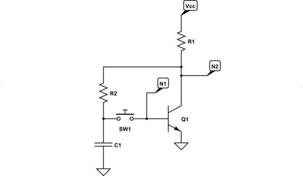
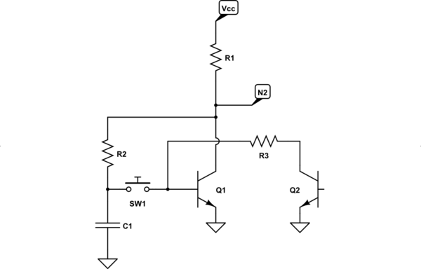
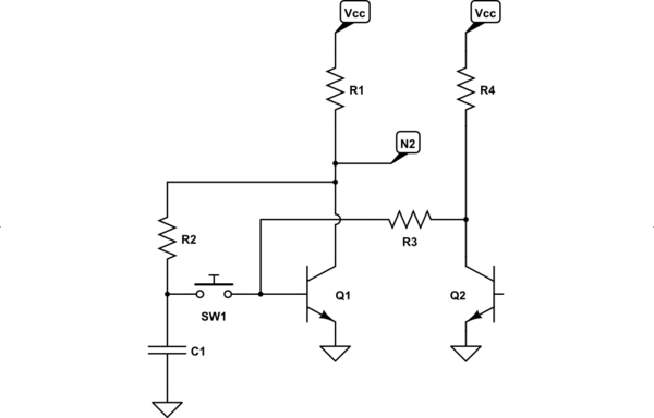
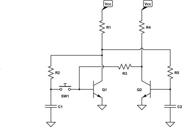
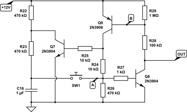
The part of the circuit that you had shown is equivalent to a two-inverter "state keeper" - a memory cell, with an additional inverter that charges a capacitor. The button connects the inverted state to the memory cell's input, flipping its state. The capacitor is driven through large resistances R22-R23, intended so that the button can be pressed for some time and the capacitor will be essentially static while that happens. The time constant of the capacitor voltage is approximately 1μ*1MΩ=1s. So, if the button is depressed for a fraction of a second, the capacitor voltage is "constant".

simulate this circuit – Schematic created using CircuitLab
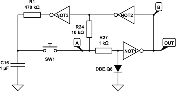
Now, we can derive an equivalent circuit that highlights the functional blocks and hides their implementation somewhat.

simulate this circuit
Alas, the overall approach is problematic. We don't want the circuit to be sensitive to the duration of the button press. The memory cell's input should be driven momentarily only, no matter how long the button is depressed. Every time the button is depressed, there should be a positive or negative pulse sent to the input, to flip it.
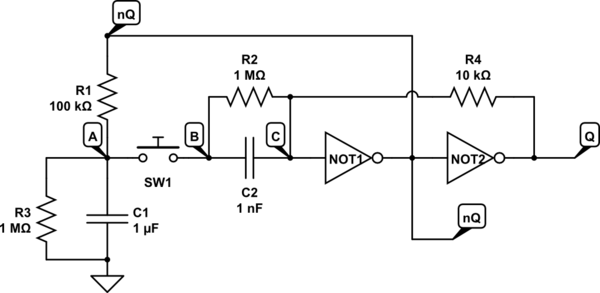
We can generate such pulses using a differentiator. So, something like the below:

simulate this circuit
The overall idea is rather simple: C1-R1 forms a low-pass filter that slows down the rise and fall times of the output nQ, so that they don't reach the memory cell input C. Since the differentiator's time constant C2*R2=1ms is much smaller than C1*R1=100ms, the slow changes of the voltage on A are not passed to C.
C1 is discharged via R3, so when the power is lost for more than a second or two, the startup condition will revert to OFF. Short power interruptions will maintain the previous state. This is - presumably - desirable.
When the button is open, both sides of the differentiator capacitor C2 are at the same potential, since it's shorted via R2. C1 is charged to the inverse of the output logic state. When SW1 is depressed, the inverse state on C1 is passed through C2 to the input of the memory cell, flipping its state. After a couple ms, C2 charges up and becomes "open circuit". Further changes of voltage on C1 are slow and cause only small voltage changes on the differentiator output - too small to change the state of the memory cell.
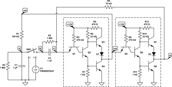
What's left to do is to implement it using transistors. To make the circuit robust, the inverters need to have push-pull or totem-pole outputs with impedance much lower than whatever we connect as a load. Ideally, we'd also want the circuit to consume very little power when idle, to make it useful on battery power.

simulate this circuit
Each rectangle is a TTL inverter, scaled for 12V operation. The resistor values may need to be adjusted to be more in the center of operating range.
Now we can work on making it consume less power. Using CD40106 as inverters would solve that issue pretty much.


