9
\$\begingroup\$

I am quite new to learning op-amps.

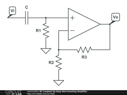
What is the purpose of putting R1 there? Does this have any meaning in the design of a microphone amplifier?

I read about this from another answer, which says that the resistor provides a low input impedance for the opamps. Why is it needed? My professor also says that it is related to "minimizing the loading effect". What does it mean? How should I decide on the value?

enter image description here

\$\endgroup\$
5
  • 2
    \$\begingroup\$ We need to provide a path for a non-inverting input bias current. electronics.stackexchange.com/questions/320300/… Also the capacitor we need a path for charging and discharging current as well. \$\endgroup\$
    – G36
    Commented Jan 30, 2023 at 15:53
  • 3
    \$\begingroup\$ R1 is part of the AC coupling high-pass filter, not strictly necessary for a non-inverting amplifier in general. \$\endgroup\$
    – Hearth
    Commented Jan 30, 2023 at 15:55
  • \$\begingroup\$ ryan, Please give us some feedback. Do you see now why there has to be a capacitor charging/discharging current path and an "input bias current" path? \$\endgroup\$ Commented Jan 30, 2023 at 21:11
  • \$\begingroup\$ @ryan Also pay attention, that your input is AC-coupled, but your amplifier applies gain to both AC and DC parts. By that i mean, if you willing to use single power supply, you should provide offset for "+" input, which is usually Vsupply/2. To remove DC gain, place capacitor in series with R2, according to rules ErnestoG mentioned. \$\endgroup\$ Commented Jan 31, 2023 at 6:10
  • \$\begingroup\$ I have a link to an MIT lecture note that I have learned a good bit from. It is not exactly an answer for this question, but I still think you might gain from reading it: "How to bias an op-amp": ocw.mit.edu/courses/… \$\endgroup\$
    – Frodyne
    Commented Jan 31, 2023 at 9:06

6 Answers 6

20
\$\begingroup\$

It's for biasing the (+) input. If it's not there, then the bias current of the op-amp will have no where to go and the voltage at that node will drift.

This RC combination forms a bit of a high-pass filter. You want to define such that the -3dB frequency is less than your minimum signal frequency (for audio 20hz approx.).

In addition, the bigger this resistor the smaller its contribution to the input-referred noise. However, you have to find a compromise because the input bias current also develops a drop across this resistor and can contribute to offset (simply ibias*R).

If you want to prove to yourself how the noise of this resistor contributes to your input referred noise (and how it is made insignificant), you can check my other answer here.

In short, the input-referred noise contribution due to \$R_1\$, assuming a input source resistance of \$R_s\$, is simply given by: $$ V_{n,R_{1}}^2 = \frac{4kT}{R_{1}}R_s^2 + \frac{4kT}{R_{1}}\left(\frac{1}{\omega C}\right)^2 $$ EDIT:

My professor also says that it is related to "minimizing the loading effect".

R1 doesn't have anything to do with any "loading effect " if it is large (perhaps \$>100k\Omega\$). If it's small, on the other hand, then it will start loading the source impedance of your input voltage source.

\$\endgroup\$
7
\$\begingroup\$

What is the purpose of putting R1 there?

Two devices need R1 - the input circuit (because of the charging of the capacitor) and the op-amp (because of the input bias currents). There is no connection between the two tasks; R1 serves them both. Let's start by considering the input circuit need.

Why does the input circuit need R1?

In AC amplifiers, it is often necessary to "move" voltage variations to an appropriate level for processing by electronic devices (op-amp here). This operation is known as "biasing". This role is performed here by the CR1 network.
A non-inverting amplifier has a very high input resistance, so in the circuit diagrams below we will assume it is an open circuit ("nothing").

AC input voltage

In the simplest case, an AC signal "wiggles" around the zero voltage level (ground).
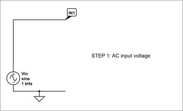
schematic

simulate this circuit – Schematic created using CircuitLab

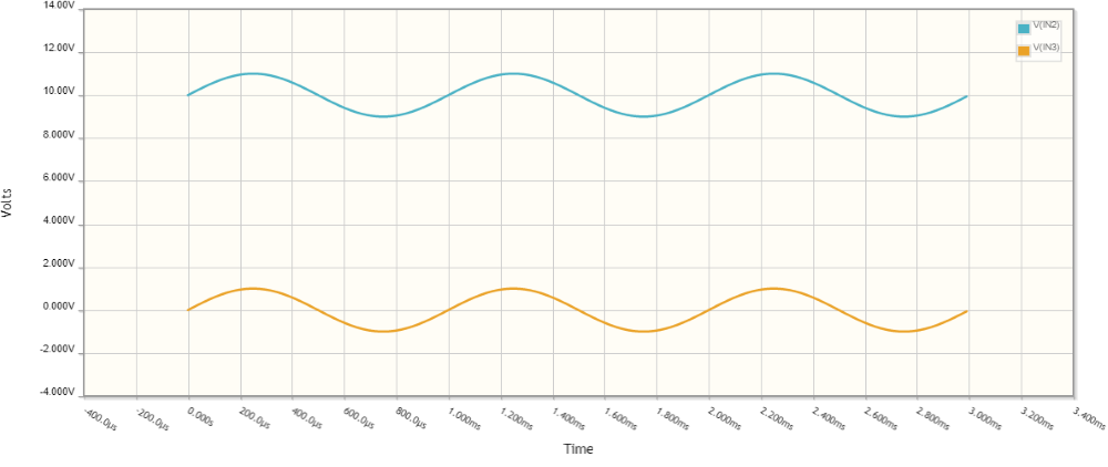
AC+DC input voltage

In many cases, however, the AC voltage is "shifted" by a constant value. For example, in the figure below Vin is "lifted" with Vref (i.e., the two voltages are summed according to KVL). In this case, this is implemented as a DC source connected in series to the AC source.
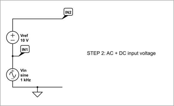
schematic

simulate this circuit

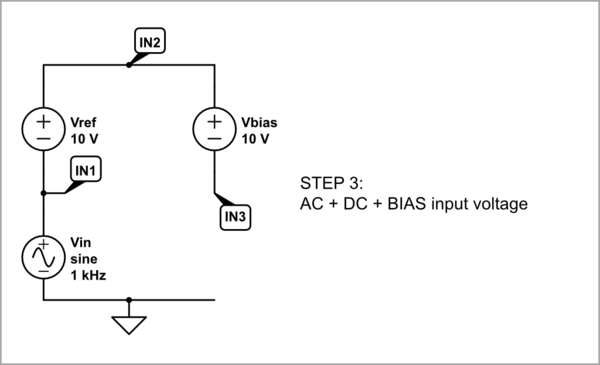
AC+DC+BIAS input voltage

This requires the input circuit of the amplifier to "shift" (bias) it back to zero. In our example, this means subtracting the bias voltage from the total input voltage and the resulting voltage (Vin + Vref - Vbias) to be applied to the op-amp input. We can implement it as above by connecting a DC source Vbias in series and in opposite direction to Vref.
schematic

simulate this circuit

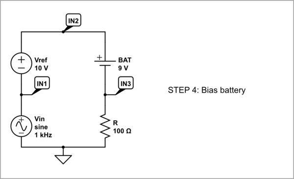
Bias battery

But this voltage source is "floating"; so we can implement it with a battery. And an ordinary battery would do the job, but for it to work for an unlimited time we need to put a rechargeable battery. It has to be charged from somewhere; so we close the circuit with a resistor.
schematic

simulate this circuit

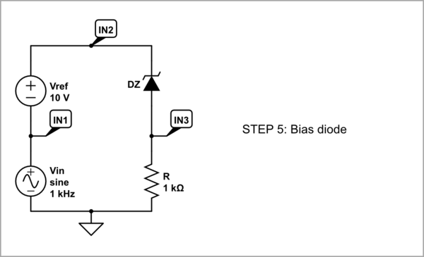
Bias diode

Any device that can maintain a constant voltage would work here. For example, it can be a diode (ordinary, LED, Zener, etc.)... but this has some peculiarities. The problem is that the Zener diode is not a source; so when Vin reaches the ground, the voltage across the diode becomes zero... the current stops flowing through it and it stops working. To solve this problem, the resistor must be connected to a negative source.
schematic

simulate this circuit

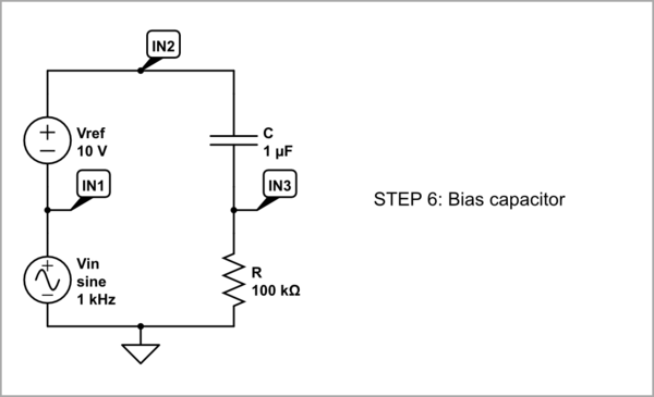
Bias capacitor

The most convenient devices for this purpose have turned out to be capacitors, and therefore historically they were the first to be used in AC amplifiers. To understand them, we can think of them as some kind of "rechargeable batteries". Here is the circuit operation...
schematic

simulate this circuit

CR - Fig.6

Vin = 0. Initially, the capacitor is charged through the resistor to Vref (like the rechargeable battery above). The current flows through Vref, C, R, ground and Vin (zero voltage). At the end of charging, Vc neutralizes Vref and the total voltage in the loop is zero; so the current stops flowing.

Vin > 0. During the positive half wave of Vin, only it acts in the loop. A current flows from Vin, Vref, C, R to ground. As a result, the positive Vin appears across R as an op-amp input voltage. The capacitor slightly charges.

Vin < 0. During the negative half wave of Vin, a current flows from Vin, ground, R, C and Vref. The negative Vin (below the ground) appears across R as an op-amp input voltage. The capacitor slightly discharges. It is interesting that the capacitor acts as a source producing the discharging current.

Thus, the voltage across the capacitor fluctuates slightly but its average value remains relatively constant. An advantage of the bias capacitor is that its voltage is always equal to Vref even when it changes over time for some reason.

"Coupling" vs "decoupling"

In these applications, the main property of voltage-stabilizing devices (voltage sources, diodes and capacitors) to maintain a constant voltage across themselves is exploited.

Coupling capacitors. When they are "floating" and connected in series (as a bridge) between the output of the previous stage and the input of the next stage, their output terminal follows the changes of their input terminal, i.e., they "shift" the input voltage. As they say, the two stages are "coupled" through them.

Decoupling capacitors. When they are usually grounded and connected in parallel (as a shunt) to some device (e.g., a weak power supply), the voltage of their ungrounded terminal does not change, i.e., they fix the device voltage. As a result, all devices connected in parallel do not influence each other through the supply voltage... they are, as they say, "decoupled".

Here is another example (my picture) of using these techniques in AC transistor amplifiers where coupling capacitors (C1 and C2) and decoupling capacitor Ce are represented as shock absorbers (mechanical analogy). C1 "shifts up" the input voltage and C2 "shifts down" the output voltage.
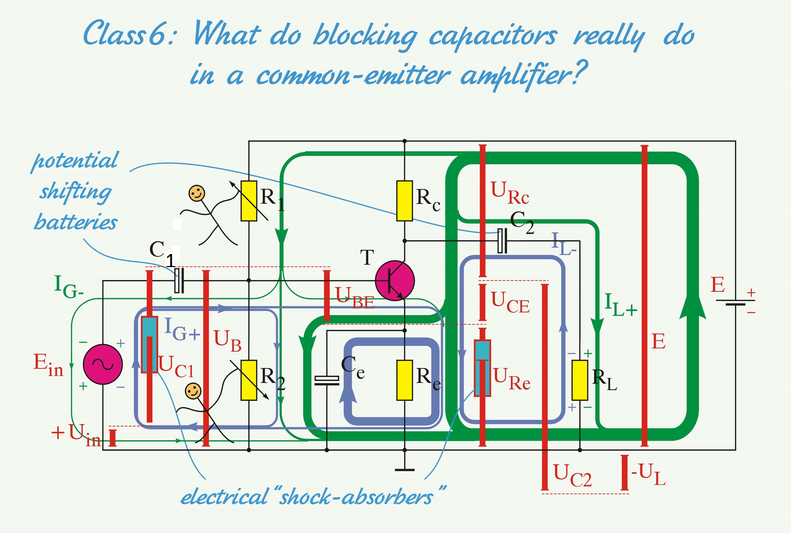
AC transistor amplifier

Why does the op-amp need R1?

Now let's see what the op-amp need is. It is related to the op-amp input bias currents.

Input bias currents

One of the most misunderstood things about op-amps are the so-called "input bias currents". Where do they come from? Why should we provide them with a path to ground? Why are they currents and not voltages? I have tried to answer these questions as a student and later as a teacher. In the end, I was able to find the answer... and now I am going to share it with you. Here is my story...

Biasing from the base side

"Biasing" basically means adding another "input" signal to the real input signal. The classic way this has been done for many years is "by voltage" and "from the base side" (from the input side of the transistor). Then we clearly see how the two voltages - bias and input - add up and their sum is applied to the base. Examples of this are the complementary output stages of amplifiers.

Biasing from the emitter side

In op-amp input differential stages, however, this is done in a strange way - "by current" and "from the emitter side" (from the output side of the transistor). Let's see how it is done in the circuit below. It is split supplied with two identical power sources connected in series; the midpoint serves as ground. The upper source +V is connected with its negative terminal to ground so that its voltage is positive with respect to ground; the lower source -V is connected with its positive terminal to ground so that its voltage is negative with respect to ground.
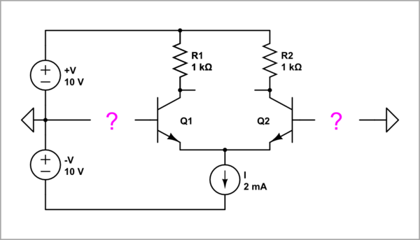
schematic

simulate this circuit

A bias constant current source is inserted into the emitters of the transistor pair (between the emitters and the negative power supply). It forces the transistors (by the negative feedback mechanism) to adjust their base currents to let this emitter current pass through them. These base currents come out of the negative source, then exit the ground and have to go through somewhere to enter the base.

Let's now examine a 1/2 differential amplifier (the left half of the circuit diagram) at three different input elements by observing whether the base current changes.

Input ground. It is easiest to just connect the base to ground. The bias current source encounters no resistance and easily drives the base current through the short circuit.
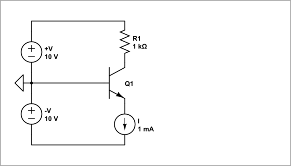
schematic

simulate this circuit

Input voltage source. Circuit designers have made an unusual decision - to insert the input voltage into the current path. Obviously, the point of this trick was to get the maximum input resistance possible. However, this requires that the input voltage source must always be connected and that it must be galvanic (pass DC).

The current source is forced to increase its voltage to compensate for the disturbing effect of the input source. As a result, the base current hardly changes.
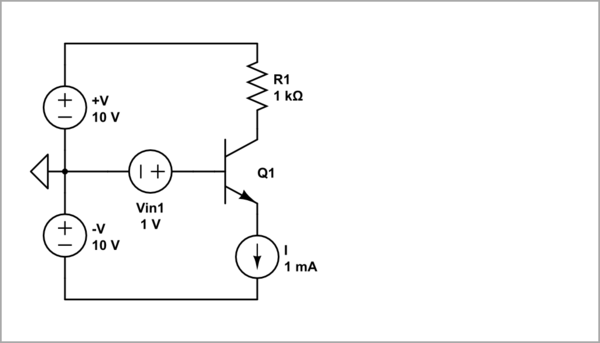
schematic

simulate this circuit

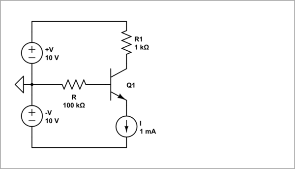
Input resistor. When the input voltage source is not "galvanic" (as it is here), we have to close the circuit (with the resistor R). The problem is that this element appears in parallel with the input source and draws a current from it (it is something different from the "input bias current"). So the op-amp input resistance decreases.

The voltage drop across R is small and the current source easily compensates for it; the base current hardly changes.
schematic

simulate this circuit

From the simulations above we see that in all three cases the base current is almost the same. So, since the input bias currents are set by a constant current source, their paths can be closed by any elements as long as they are "galvanic".

"Inventing" the differential pair

Here comes a unique opportunity to see a possible way how to "invent" the legendary "long-tailed pair"... and I will take advantage of it.

But it does not amplify!

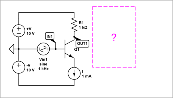
Unfortunately, there is a "little" problem with our "half differential amplifier" - it is not an amplifier:-) Let's check this speculation by applying an AC input voltage with significant magnitude and observing the output voltage at the collector.
schematic

simulate this circuit

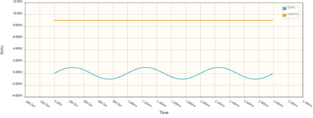
The result confirms our suspicions - even when the amplitude of the input voltage is 5 V, the output voltage does not change. What is the reason?
DA_outlined - graphics-5

The problem is that because of the current source, the emitter voltage is not fixed but changes simultaneously with the base voltage. Obviously we need to "immobilize" the emitter with something... but what should it be?

Figuratively speaking, the current source is extremely "soft", the resistor less... and the voltage source is absolutely "stiff". So we need something like a voltage source.

Assembling the full differential pair

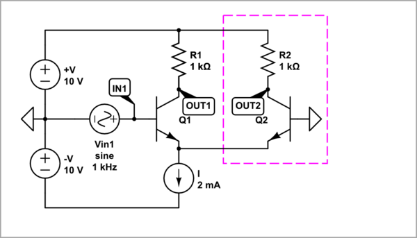
Eureka! It can be another transistor connected as an emitter follower (the right half of the differential pair).
schematic

simulate this circuit

The result is impressive - only 50 mV cause 1 V output voltage!
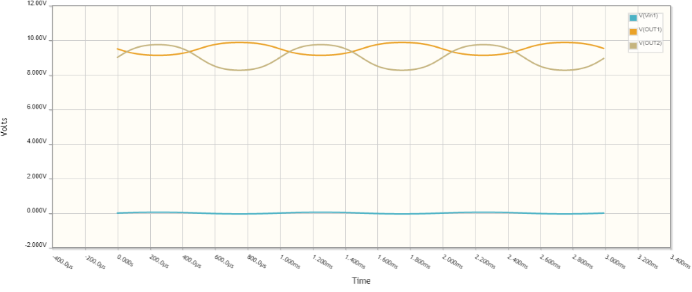
DA_outlined - graphics-6

Now all that remains is to connect a second input source to the Q2's base to get the beautiful symmetric differential pair...
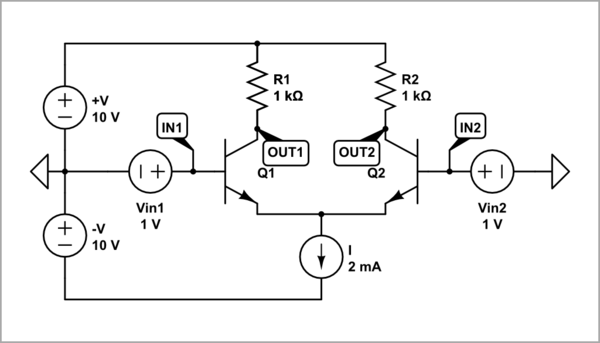
schematic

simulate this circuit

Play with the circuit by changing the input voltages in various ways:

Vin1 = Vin2 = +const (static common mode)
Vin1 = Vin2 = -const (static common mode)
Vin1 = +var, Vin2 = +var (varying common mode)
Vin1 = -var, Vin2 = -var (varying common mode)
Vin1 = var, Vin2 = const (asymmetric differential mode)
Vin1 = const, Vin2 = var (asymmetric differential mode)
Vin1 = +var, Vin2 = -var (differential mode)
Vin1 = -var, Vin2 = +var (differential mode)...

\$\endgroup\$
6
\$\begingroup\$

Assuming ideal components, R1 works with C as a high-pass filter.

Select R1's resistance such that \$f_{corner} = \frac{1}{2\pi{}R_1C}\$. Your microphone probably has a lower frequency limit; this is a good corner frequency to design for.

Without it, the op amp will amplify any DC component in your circuit, with unpredictable results.

Since we have non-ideal components, R1 also provides a path for input bias current. All op-amps draw a small amount of input current (sometimes picoamps) but it needs to come from somewhere.

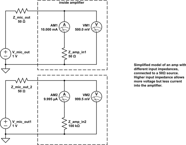
Regarding the loading effect edit: your professor is talking about the fact that a sensor's output voltage can be meaningfully changed by a low-impedance input on the downstream device. While a sensor/transducer will produce an analog voltage proportional to some real world value, it's not a perfect voltage source and has some output impedance. If the output impedance of the sensor is high enough, and the input impedance of the downstream device (e.g. amplifier or controller) is low enough, the system behaves like a voltage divider, giving you an output different from the true value.

schematic

simulate this circuit – Schematic created using CircuitLab

In your example, if R1 is low enough, it'll pull the microphone's output too strongly towards ground, attenuating the input signal. But since an op-amp is a voltage-controlled device, you want to have as much voltage as possible at its input. A low R1 impedance will just make your signal quality worse.

\$\endgroup\$
6
\$\begingroup\$

For a classic non-inverting opamp circuit, the action of negative feedback is to do whatever is necessary to drive the inverting input such that the voltage difference between the inverting and non-inverting inputs is zero volts. (Technically, near-zero volts, but zero is good enough for now.)

IOW, negative feedback drives the - input to equal whatever is the instantaneous voltage at the + input. Note that this voltage does not have to be GND. If R1 is connected to a 2.3 V voltage source of some kind, then the output will try to be 2.3 V times the circuit gain.

For an AC-coupled input, there is no explicit reference potential to set the operating point of the circuit. An audio signal might be 100 mV, but the cap could be charged up to 50 V. Theoretically, the opamp input is an infinite impedance so it sees 50.1 V and tries to deal with that while running on 12 V, 15 V, whatever.

Hence, R1. It establishes a DC operating point for the signal system, and provides a discharge path for C in case the input is connected to a signal with a non-zero DC component. The larger R1 is, the more susceptible the circuit is to radiated noise. The lower it is, the more it loads the input signal source, possibly reducing the input signal seen by the opamp enough to matter. Life is choice.

Update: To be clear, loading is a very real thing. The signal source output impedance plus the C impedance (at any particular frequency) sum to form the series leg of a voltage divider. R1 is the shunt leg. Thus, how much R1 loads the signal source can be calculated with the capacitor impedance equation and Ohm's Law. Separate from that, R1 and C form a high-pass filter.

One way to calculate things is to start with a value for R1 that is high enough not to load the input beyond an acceptable level. Next, select a corner frequency for the high-pass filter, and calculate the value of C using that frequency and the value of R1. Finally, adjust the component values for commercially available parts, things you already have in inventory, etc.

\$\endgroup\$
2
  • \$\begingroup\$ Something else to consider is the time constant of the RC filter which will affect the time for stabilization of the output signal, when a signal with a DC component is applied to the input. \$\endgroup\$
    – PStechPaul
    Commented Jan 31, 2023 at 22:05
  • \$\begingroup\$ It'll be susceptible to radiated noise, imo, only if the source impedance is big. If not, you'll always have a low impedance node there since it's the parallel combination of Rsource and R1 that counts. \$\endgroup\$
    – Designalog
    Commented Feb 1, 2023 at 5:38
5
\$\begingroup\$

If you removed both C and R1, and connected the source signal directly to the opamp's non-inverting input, the amplifier would work perfectly well. However, if the input signal has any non-zero DC offset (ie. it fluctuates above and below some non-zero mean) that DC offset would also be amplified, and appear as a large offset in the output. In other words, if the gain of the amplifier is \$1+\frac{R_3}{R_2}\$, and the input signal is offset (centered around, has a mean of) +5V, the output signal from the amplifier stage would be centered about \$5 \times \left(1+\frac{R_3}{R_2} \right)\$, not 0V. That could be quite a big offset, easily near/beyond the power supply potentials, which would cause clipping.

One purpose of the pair C and R1 is to "shift" the input signal to become centered about 0V by the time it reaches the amplifier stage, so the amplifier output is also centered about 0V. This technique is called "AC coupling". It works because capacitor C eventually charges to some steady DC voltage (the average value of the input signal), which when superimposed on the input effectively "offsets", or "shifts" it back to zero mean. Essentially, the potential at the right side of the capacitor becomes some DC-offset copy of the signal potential on its other side. Now the amplifier stage sees a signal which swings above and below ground potential.

You could consider the purpose of R1 in this scenario to be to provide a "loose" connection to whatever potential you wish that average (or mean, or centre potential) to be; zero volts in this case. The potential at the top terminal of R1 is free to wobble up and down because it's not tied directly to ground, but the presence of a fixed potential at its bottom terminal determines the mean, "center" value about which the signal oscillates.

For example, if you desire a signal which fluctuates above and below a mean of +10V DC, simply connect the lower terminal of R1 to a fixed voltage source of +10V. In this case, the amplifier stage is expecting a zero-average signal, so the bottom of R1 is grounded.

To summarise all that, you could say that capacitor C removes any DC offset from the source signal, by introducing an opposing DC offset of its own, and resistor R1 "biases" the right side of C to whatever mean potential you desire.

Your professor hinted that this combination of C and R1 present a "load" on the source signal, which may or may not be desirable, depending on the ability of the source to overcome ("drive") that load. Larger C or smaller R1 would be a heavier load. Considering that without C and R1 the input to this system would be the op-amp's non-inverting input (which could be gigohms), C and R1 can only lower overall input impedance. I don't understand the meaning of your phrase "minimize input impedance"; rather I would say that C and R1 actually set the input impedance, as seen by the source, since the op-amp's own contribution is negligible in comparison.

C and R1 together form a filter, and their values together determine the cut-off frequency. That maybe another reason why R1 (and C) is there; performing the function of removing any AC components below some explicitly chosen minimum frequency. Note that this includes zero-hertz, otherwise known as DC! You can perhaps see why my above explanation of DC offset removal would be perfectly in keeping with this "high-pass" filter behaviour.

You would need to choose values of R1 and C that provide loading (input impedance) appropriate for the source, and a cut-off frequency that doesn't chop out any desired components of your signal. In the context of microphone amplifiers, where noise is an important consideration, low resistances are better, but too low a resistance for R1 will draw more current from the source, and may excessively attenuate or even distort the source signal. If R1 is too high, thermal noise might become an issue.

Whatever values you choose, the cut-off frequency of this filter stage shouldn't be so high that you lose bass components of the audio signal. Ultimately these values will be some compromise that will perform DC offset removal (AC coupling), without also killing off any low-frequency audio components you require in the output, without excessively loading the source, and without introducing excessive thermal noise.

\$\endgroup\$
0
1
\$\begingroup\$

In order to balance the input impedances, you need to aim R1 = R2//R3.

\$\endgroup\$

Your Answer

By clicking “Post Your Answer”, you agree to our terms of service and acknowledge you have read our privacy policy.

Not the answer you're looking for? Browse other questions tagged or ask your own question.