0
\$\begingroup\$

I am trying to understand exactly how the stages of this Moog high-pass filter work but I still have several things that I cannot quite figure out:

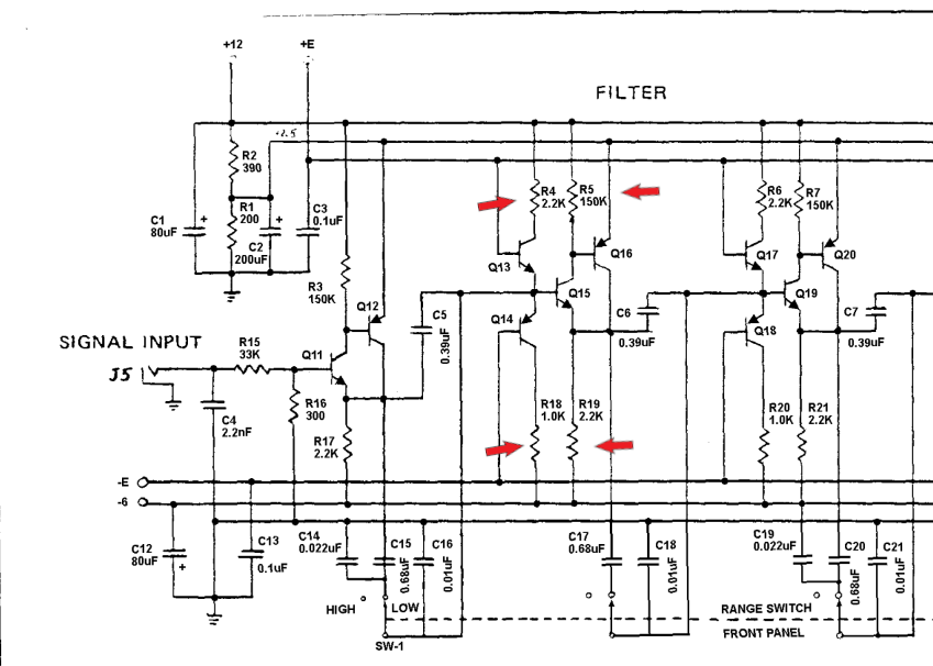
One stage of the Moog high-pass filter for small signal audio

  1. Q13 and Q14 form a push-pull amplifier, and are biased with a 450mV - 650mV voltage (for Q13) and -450mV - -650mV (for Q14). What is the purpose of the 2.2k and 1k resistors in the collectors of the BJTs? I cannot seem to find other push-pull amplifier schematics with collector resistances. How are the resistor values calculated?
  2. Is the purpose of the push-pull pair to create a voltage controlled variable resistor, and then in conjunction with the C5, C6 etc capacitors to form a passive high pass filter stage? If so, in a passive high-pass filter, isn't the resistor supposed to be going to ground or at least to a lower potential?
  3. Q15 and Q16 form a Sziklai/complementary feedback pair. Is the pair used as a voltage buffer? Why use Sziklai and not a single NPN?
  4. What is the purpose of R5 and R19 in the Sziklai pair? How are the resistor values calculated?
\$\endgroup\$

2 Answers 2

0
\$\begingroup\$

Q15 and Q16 are simply forming a buffer with an enhanced gm, such that its transfer gets much closer to 1.

I don't think Q13/14 are a push pull amplifier, unless there's a signal present at that E terminal.

My best guess is that they are implementing an active voltage divider because the node voltage on the right side of C5 would be undefined without it. The resistors have probably been sized to accommodate the swing at said C5 right side node such that Vce of both transistors are not small and turn off.

\$\endgroup\$
0
\$\begingroup\$

If the E rails are very low voltage (and probably logarithmic to some control value, and temperature compensated), they are probably being used to adjust the emitter impedance of Q13/Q14. R4/R18 are then just current limiting resistors, only coming into play when overdriven. (When Q13/Q14 saturate, the E rails will be dragged down a bit; probably this is avoided by keeping signal and E voltages nominal.) This would allow an adjustable highpass effect in the snippet shown. Or perhaps a phase shift effect, such as for a variable oscillator (if looped through a voltage gain stage). The signal level also needs to be small for this to be effective (without significant distortion), 10s of mV.

They also provide bias for the buffer stage.

R15/R16 makes ~1/100 the input, so if the input is line level (fractional to a couple of V), this checks out. Q11/Q12 are then biased with R16, which doesn't need to be adjustable so a resistor is fine.

The input buffer must be necessary to get a low drive impedance for the following stage; since Q13/Q14 impedance can be quite low (10s Ω near saturation). This implies the gain as well as cutoff frequency will vary; probably the E rails are kept low enough so that these impedances are modest (~kΩ), keeping passband gain near 1.

\$\endgroup\$

Your Answer

By clicking “Post Your Answer”, you agree to our terms of service and acknowledge you have read our privacy policy.

Not the answer you're looking for? Browse other questions tagged or ask your own question.