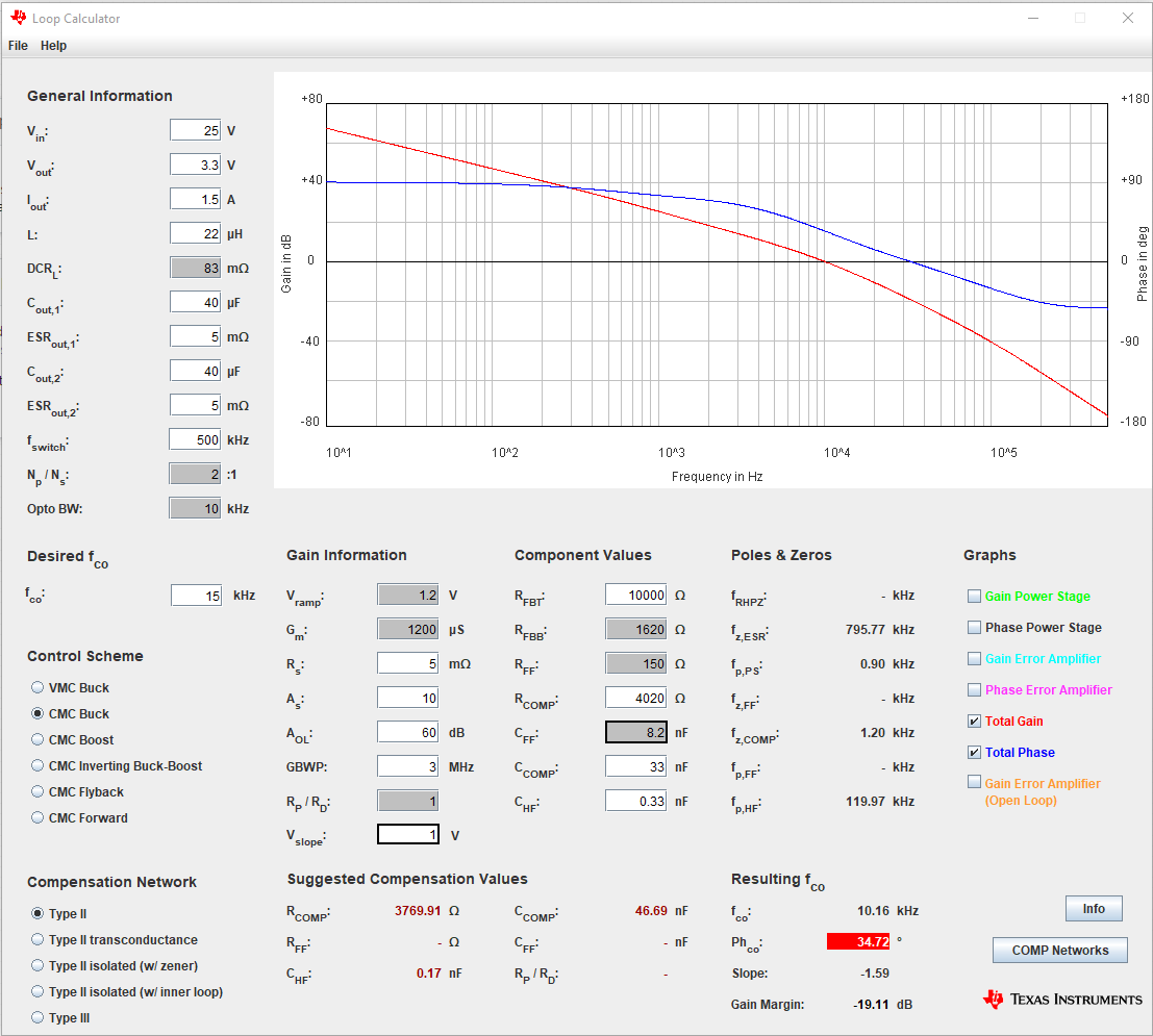
I will try to give you here a very brief overview of the principles at work here. The tool you show is intended to stabilize a closed-loop switching converter such as a buck, boost or buck-boost if we talk about the basic switching cells.
If I take the simple case of the buck, the converter is intended to deliver a stable output voltage, e.g. 5 V from a 12-V source, regardless of the input voltage and the output current absorbed by the load. The buck alone - without feedback - is affected by an output resistance \$R_o\$ and delivers an output voltage directly proportional to \$V_{in}\$. If I purposely exclude all drops incurred to other contributors (\$r_{(DS(on)}\$, diode \$V_f\$ etc.), we have \$V_{out}=DV_{in}-R_oI_{out}\$. In this expression, \$D\$, represents the duty ratio and is the control variable. Whether the cell operates in voltage- or current-mode control, \$D\$ has always the same value for a given operating point and sets the output voltage.
From this simple expression, you realize that if your load draw more or less current or if the input source varies, the output voltage will be affected and regulation may be lost. Here, the input voltage and the output current are the perturbations we want to reject. A feedback loop will thus permanently observe the output voltage (in this case) and compare it to a fixed and stable reference voltage \$V_{ref}\$, e.g. 2.5 V. Very often, a scaled-down version of \$V_{out}\$ is compared to \$V_{ref}\$ and this is the role of the resistive divider of ratio \$\alpha\$ you see going from the output to the feedback pin. When the two voltages are equal, meaning \$\alpha V_{out}=V_{ref}\$, the error is zero and the regulation is, theoretically, perfectly ensured. If a deviation occurs, because \$V_{in}\$ suddenly changed or the load draws more or less current, the previous expression is no longer verified and you must act on the control variable \$D\$ to bring back \$V_{out}\$ in regulation. This observation role is given to the feedback loop which will drive the control variable \$D\$, either directly as in voltage-mode control (VMC) or indirectly as in peak-current-mode control (CMC).
The loop must observe a certain polarity to perform its job well. If the regulated variable \$V_{out}\$ is too high, e.g. it exceeds the reference voltage, then the duty ratio \$D\$ must be reduced. On the opposite, if more current is absorbed and the output voltage drops, then the error voltage increases which, in turn, must bring the duty ratio up. Ensuring the correct variation of the duty ratio versus the regulated variable from dc (in static) up to a certain frequency (in dynamic) is the essence of a stable loop behavior. For instance, the loop must react quickly if a perturbation occurs but shall not be too vigorous or nervous otherwise overshoot may happen. That means that the error generated by the deviation between the observed scaled-down \$V_{out}\$ and \$V_{ref}\$ must be amplified and shaped to bring the best possible transient results.
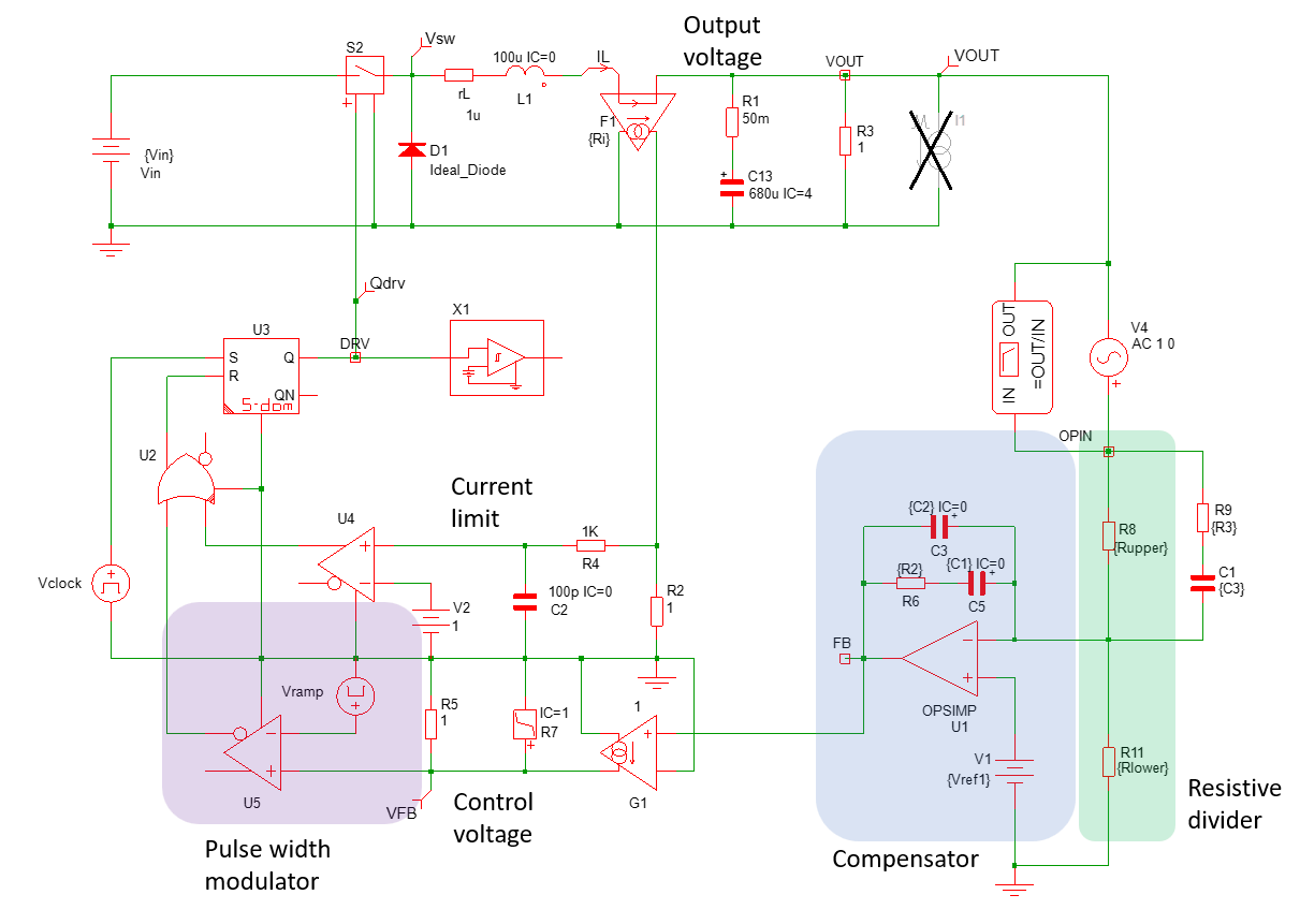
Below is a typical closed-loop buck converter which is part of my 80+ ready-made templates you can download freely from my webpage:

In this picture you see the elements I have introduced. The duty ratio is elaborated through a so-called pulse-width modulator (PWM) which compares the error voltage to a sawtooth (\$V_{ramp}\$ in the drawing). It is a voltage-mode buck converter and the current loop you see is for limiting the current in the inductor, cycle-by-cycle. The error voltage is delivered by the compensator or error amplifier highlighted in blue. That is the one you will have to work out in order to ensure regulation in presence of fast input and output variations.
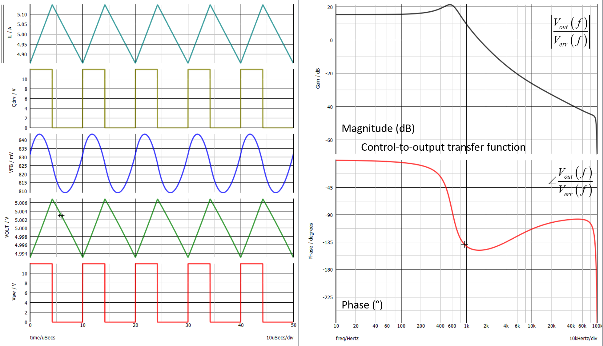
Everything starts with the control-to-output transfer function of the converter you want to control. Without it, you cannot infer a control strategy. If I apply a stimulus to the control pin, how does this stimulus propagate in the circuit to generate a response on the output used for regulation? The ratio of the response to the stimulus is the transfer function you want as a starting point. With SIMPLIS, it is easy and the Bode plot is immediately extracted from the switching circuit:

Beside SIMPLIS, you could reveal this control-to-output transfer function by the means of a mathematical relationship - see my last book on the subject for instance - or by building a prototype in the lab and use a frequency-response analyzer (FRA) for this exercise.
In simulation, always verify the operating point is correct and it is the case here with a 5-V output as expected. Now that you have the power stage ac response, you must choose a place to crossover, meaning you will shape the compensator ac response - the compensator is an active filter - to force a decrease of the loop gain and make it 1 in magnitude (0 dB) at some frequency. That frequency, noted \$f_c\$, is the crossover frequency. Before this crossover value, the converter has gain and the loop operates normally. Beyond crossover, the loop gain is less than 1 and ac feedback is gone: dc regulation is kept but the control system without gain can no longer do its job to fight perturbations. For instance, assume a 1-kHz crossover. If a 100-Hz perturbation is applied, the loop will react with the gain it offers at 100 Hz. If this perturbation is now 10 kHz, the loop no longer has gain and the converter operates in ac open loop: it will do what it can to reject the perturbation like if no feedback was present.
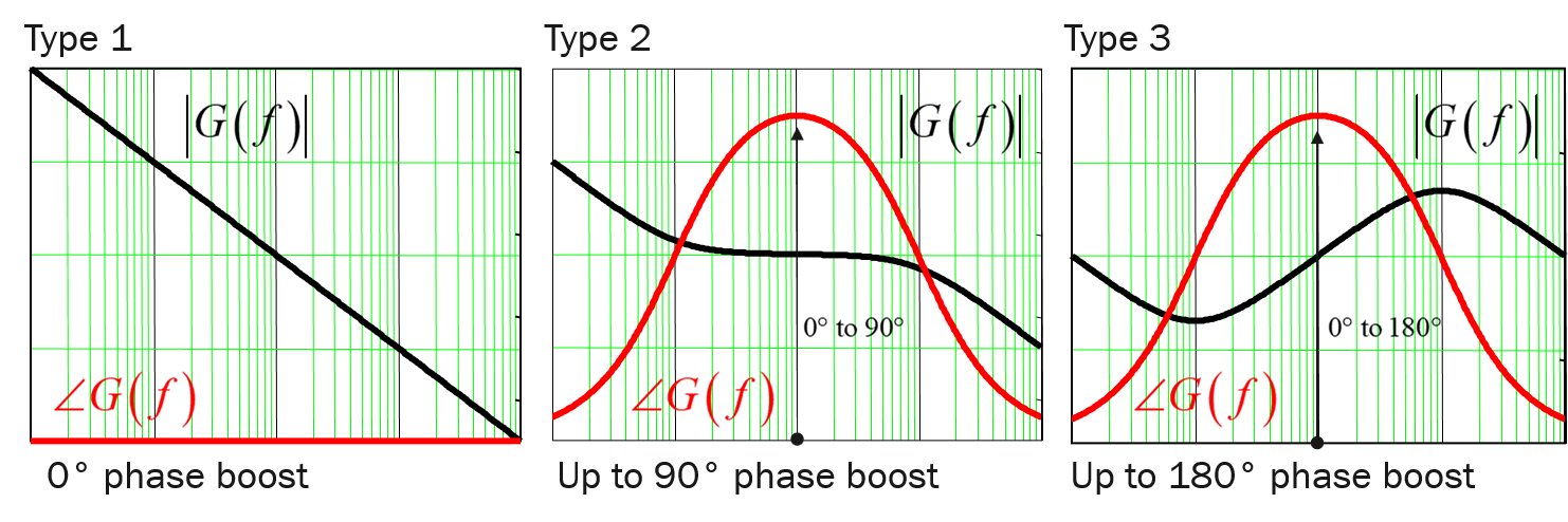
The higher the crossover, the faster the response but also the more susceptible the system can be to noise, self-generated or external. Also, pushing crossover means you expect gain from the compensation chain where the response of the error amplifier may affect the compensator response you need. I can see in the TI tool that you can enter the characteristic of the op-amp and this is good. The compensator is thus the place where you implement your compensation strategy, like placing poles and zeros to shape the response. The compensator role is to force crossover but also to provide phase boost at crossover to make sure you have the phase margin you want. We conveniently designate three compensators: type 1, 2 and 3 (see this original paper from Dean Venable).

All three compensators feature a pole at the origin to provide a high gain at dc and thus ensure the smallest error in regulation. Type 1 is a simple integrator and does offer a flat phase response. Type 2 implements an extra zero and pole and lets you boost the phase between 0 and 90°. Type 3 assembles a double pole-zero pair and gives the ability to adjust the phase boost between 0 and 180°. A type 3 is identical to a filtered PID to which an extra pole is added.
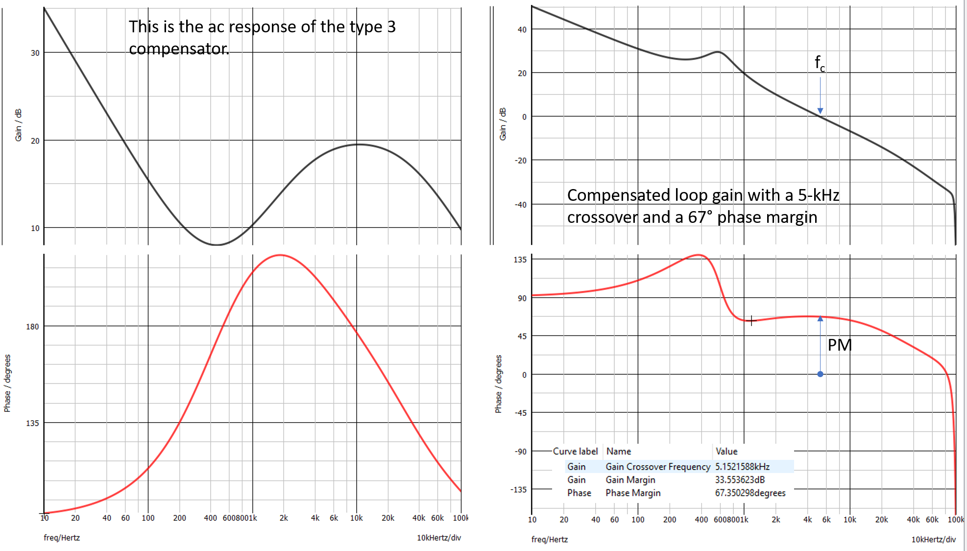
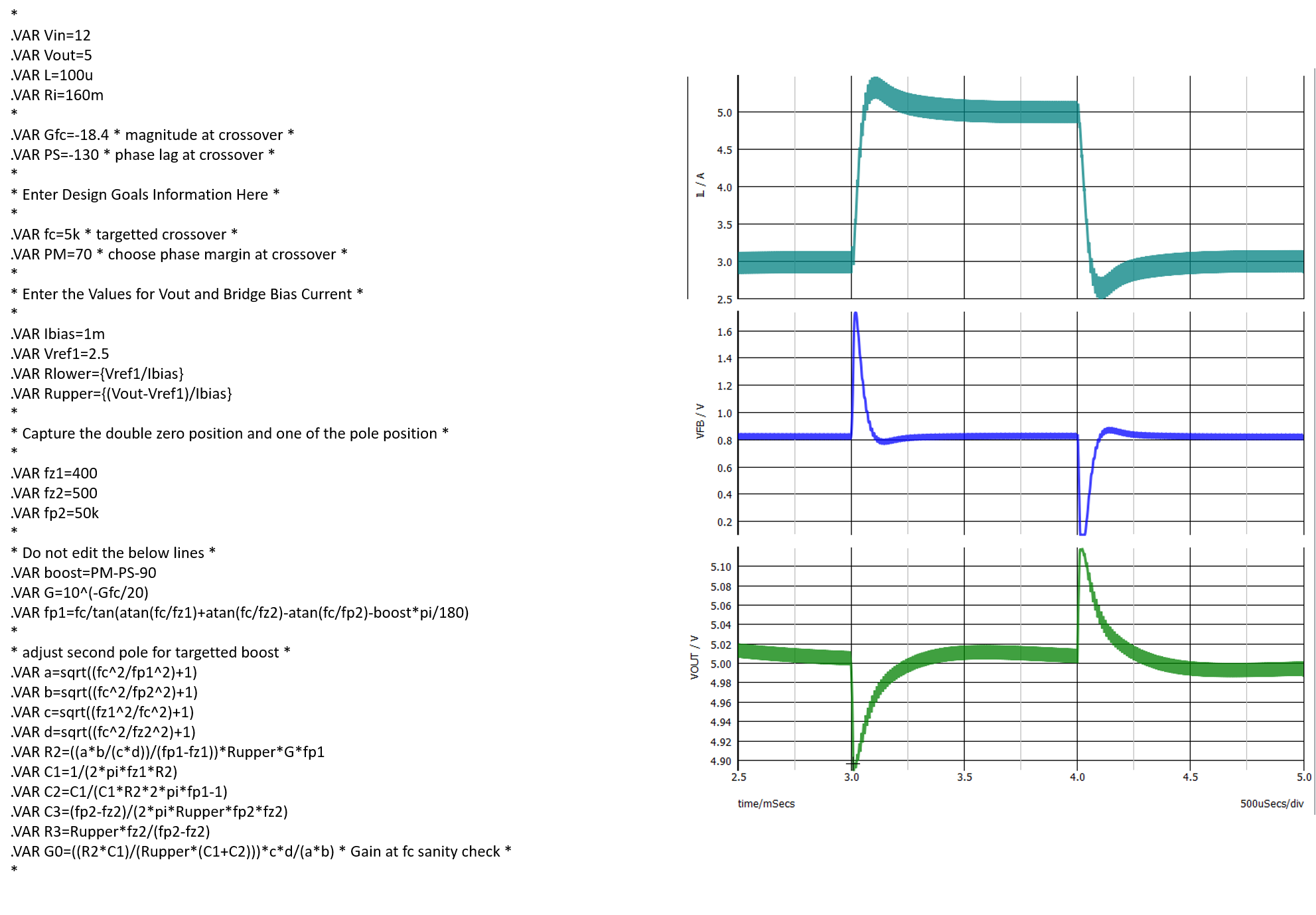
You can have a look at my APEC 2021 seminar in which I give more details but loop compensation is a vast topic. If you look at the Bode plot I gave, you see a resonance at around 600 Hz. This is the \$LC\$ network of the buck converter. The phase lag is maximum at this point and the speed at which the phase drops depends on the quality factor. To fight this double pole, I will place a double zero - a zero pair - at 600 Hz. Practically speaking, you may want to place one zero at 600 Hz and the second at a lower frequency to avoid a so-called conditional stability situation when the converter operates in light load but this remark is off-track for now. A pole with then be placed to tailor the phase margin at the wanted value, 70° in my case, while the second pole will be placed at \$\frac{F_{SW}}{2}\$ to provide a good gain margin and ensure noise rejection. What is cool is that this process is automated in the macro I include in the template. This is what the TI tool will do for you also:

As you can see, the crossover is 5 kHz and the phase margin is 67°. We can conclude this exercise by running a transient step and see how the output reacts:

The response is acceptable with reasonable undershoot. Once you are there, you must verify the loop remains stable in all possible operating conditions but also that its performance will remain acceptable during the lifetime of the converter, enduring all possible components variations such as capacitor ESRs for instance. Monte Carlo analysis is a possible tool for checking how crossover and phase margin will resist to components tolerances for instance.
This is all I can write on a Saturday morning. It is obviously an incomplete picture but there are plenty of sources in the literature, in books or online to dig the subject further. For now, time to prune my vines : )

