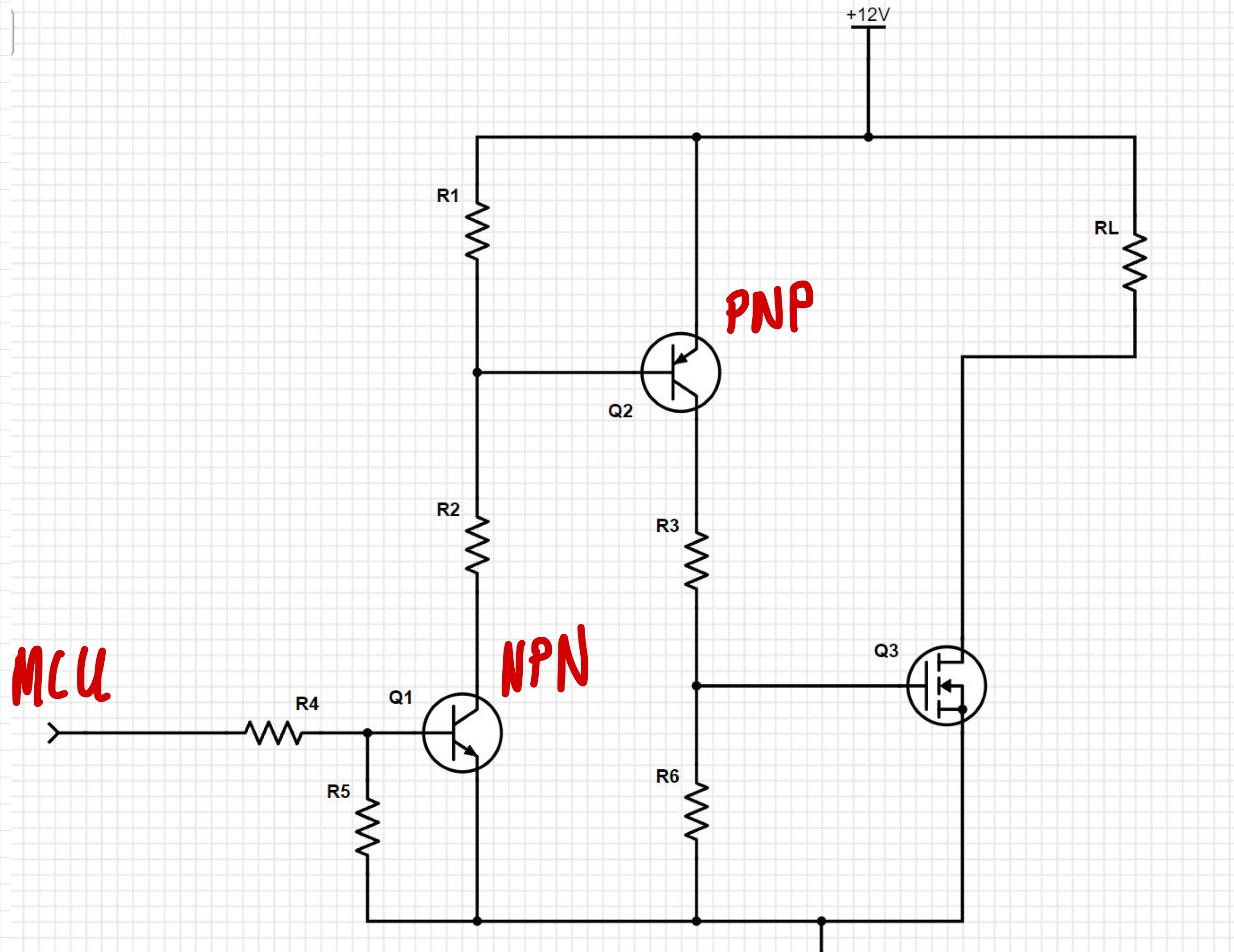
Simply, you can get a faster rise-time this way. Whether that's important, depends on the MOSFET, what kind of load is attached, and how fast it should be switched.
Conversely, the single-NPN version has fast fall-time and slow rise. Or vice-versa if a P-ch MOSFET is used (given some other considerations: performance is generally ~2.5x poorer than NMOS, and assuming the load can be common-ground instead).
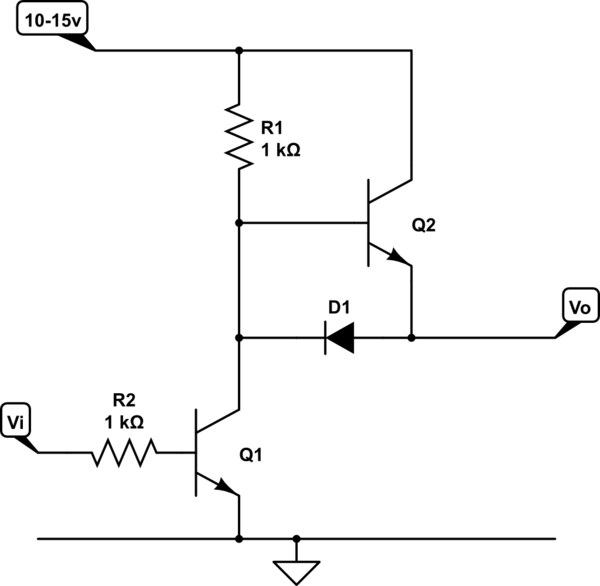
We can address these by "boosting" the pull-up/down resistor with an emitter follower:

(Resistor values are unimportant.) Note that when Q1 is off, the equivalent circuit is R1 supplying Q2 base. Base current depends on the voltage drop from +V to Vo, and emitter current is about hFE times larger (and shifted down a VBE). Basically the emitter looks like an hFE times smaller pull-up resistor, for no cost to Q1's on-current -- efficient.
This is roughly equivalent to the NPN + PNP case, though it saves a BOM item (fewer unique parts are required).
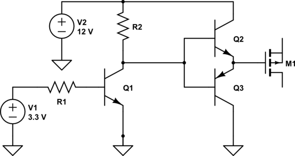
Or we can boost both ways, replacing the diode with a PNP emitter follower to boost discharge current:

This allows less current in Q1 for a given falling speed.
Note that the Q1 B-E resistor might not be needed: when the signal source is a CMOS output pin (typical these days), it has a nice low VOL, so Q1 will be discharged adequately in the low state (i.e., VBE(off) ≪ 0.7 V). (It does help with ensuring an "off" level from a tri-state source, such as an MCU during reset/initialization.) The base voltage divider motif does allow faster switching. Optimal switching is with the divider values set for a Thevenin voltage of about 2 VBE(on). So from a 5 V logic source, 10k + 4.7k is pretty reasonable for example. A speed-up cap can also be placed in parallel with the series resistor (your R4), typically 10-100 pF.
We can further improve it by replacing the pull-up resistor with a current source, so it pulls up equally as strongly across the whole voltage swing, rather than with a decreasing current.
The current itself can also be switched, to save on power dissipation, in which case the circuit starts looking a lot like a CMOS logic circuit (complementary yes, but in bipolar instead!); but then two level shifters are needed, and an inverter, and... it's a lot of components just to drive a gate, and I would definitely reach for a proper gate driver IC before going to those lengths. :)
Images from:
Driving MOSFET from MCU with BJT
Limiting the base current to BJTs in Gate Driver circuits

