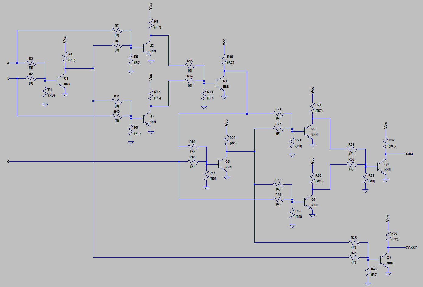
7
\$\begingroup\$

I've been trying to build some circuits that use logic gates, without using pre-made chips. My main goal is to further my understanding of the subject, but it'd be nice to make something useful in the process.

After a lot of failed attempts and googling I landed on this question, which works great. But I feel that the current consumption will be very high (since the inverters will basically send a load of current to ground when they're low?). This is especially true if you want to use many gates.

It seems to me that you need to 'black box' the logic gates so that you can chain them as much as you like without much worry. The inverters do this, but at the cost of current. Is there a better way? Is learning the hard physics behind it all the only way to really make complex logic circuits, so I'm just moving out of my depth? I have a strong understanding of the gates themselves, and designed my circuits as pure gates already, but the actual physical implementation is very different.

So my question would be: Is there a simple and effective way of blackboxing RTL logic gates so that they can be chained?

Edit: I just recalled that NOR can be used to construct other gates - so I suppose the solution would be a design for a NOR gate that can be treated as modular.

\$\endgroup\$
3
  • \$\begingroup\$ RTL goes back to the DEC PDP8 where BCD counters were $200 bitsavers.trailing-edge.com/pdf/dec/handbooks/… more bitsavers.trailing-edge.com/pdf/dec/handbooks \$\endgroup\$
    – D.A.S.
    Commented Jan 19, 2017 at 3:32
  • 2
    \$\begingroup\$ If you just want to very easily connect logic gate try CMOS ... \$\endgroup\$
    – jbord39
    Commented Jan 19, 2017 at 4:52
  • \$\begingroup\$ @jbord39 Or even NMOS. Easier to build, and power draw is limited by your choice of resistor. \$\endgroup\$
    – user39382
    Commented Jan 19, 2017 at 6:07

4 Answers 4

15
\$\begingroup\$

RTL isn't too difficult, but that doesn't mean it's trivial either. If you want, take a look at two of my answers: (1) building a full adder; and, (2) nand with led. But in those cases I decided to keep things really simple and not to actually do a serious design. You've mentioned RTL. So let's attempt an RTL design here.

Let's start out looking at the following example taken from one of my earlier posts:
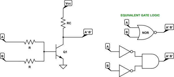
schematic

simulate this circuit – Schematic created using CircuitLab

We will need to decide upon a range of input voltages which are to be considered a logical "0" and another range of input voltages which are to be considered a logical "1". Obviously, these ranges should not overlap and probably should have a gap between them.

Before we go there, though, the above circuit presents a design problem. If we assume that both inputs (A and B) are at the highest allowable input voltage that is still considered a logical "0", then it's pretty clear that there will also be some small base current present and that this current will be amplified by the \$\beta\$ of \$Q_1\$ to become a possible collector current pulling down the collector voltage. This makes the circuit far less designable, especially because the value of \$\beta\$ varies over parts even within the same family. We need something present to make the circuit less dependent on the value of \$\beta\$. (We'll also need something to also make the circuit less dependent on the variations of saturation current [which affects \$V_{BE}\$], too. But that will shake out in the process.)

A way of achieving this is to add a resistor from base to ground (or some even lower voltage.) Something like this:
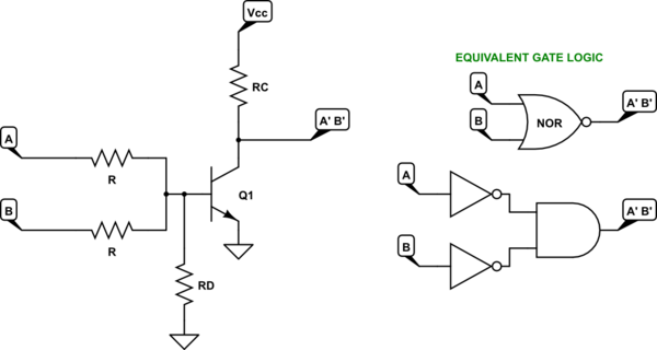
schematic

simulate this circuit

(I've shown this circuit with \$R_{D}\$ going to ground. A design could also consider the idea of tying it down to a negative rail. But there's no need, for now.)

The above circuit, with the added \$R_{D}\$ base resistor, greatly improves things as it allows us to divert small base currents away from the BJT. It provides an additional degree of design freedom that we'll find useful to have.


So. Let's design RTL!

We'll start by assuming a single voltage rail of \$V_{CC}=5\:\textrm{V}\$. Let's also say that a LOW is considered to be any voltage from \$0-1\:\textrm{V}\$ and that a HIGH is considered to be any voltage from \$3-5\:\textrm{V}\$. So, \$V_{LO_{MAX}}=1\:\textrm{V}\$ (obviously, lower is better) and \$V_{HI_{MIN}}=3\:\textrm{V}\$. Let's also say that you want the output to be able to drive up to six inputs at a time. (It is very important to set down some rules like this if you are going to design something.)

For a design, we need to figure out the worst case situations and design for those cases. (If we do that, the rest will only be better.) The two worst possible cases are:

  1. Where the two inputs are at \$V_{LO_{MAX}}\$ and the output can't be allowed to sink below \$V_{HI_{MIN}}\$ when faced with a full load of six inputs. (These additional inputs will try and drag down the output and we need to make sure that the output can't be dragged below \$V_{HI_{MIN}}\$, even then.)
  2. Where one of the inputs is at \$0\:\textrm{V}\$ and the other one is at \$V_{HI_{MIN}}\$ and where the output must be forced below \$V_{LO_{MAX}}\$ without any other output loading added. (Without added inputs, the transistor must by itself be able to pull down the output below \$V_{LO_{MAX}}\$. Adding loading would only help and we want a worst case situation where there isn't any added help.)

To address these details, I'm going to haul in a few things I know about small signal BJTs. Roughly speaking, their collector currents will increase by a factor of 10 for each \$60\:\textrm{mV}\$ change in \$V_{BE}\$. (Taking into account some reasonable thermal variations, each factor of 10 might be for anywhere from \$50-70\:\textrm{mV}\$ change in \$V_{BE}\$.)

I want \$Q_1\$ to be very close to OFF in case (1) above, setting \$R_C\$ low enough in value that it can pull up six input loads without letting the collector sink below \$V_{HI_{MIN}}\$. This means that the base voltage must be low enough to achieve that OFF state. I also want \$Q_1\$ to be very close to ON in case (2) above. This means that a slight change for one of the inputs, merely going from \$V_{LO_{MAX}}\$ to \$V_{HI_{MIN}}\$ (just \$2\:\textrm{V}\$ change), while at the same time the other input tries to oppose this change by itself going from \$V_{LO_{MAX}}\$ to \$0\:\textrm{V}\$ and dragging down against that meager rise, should be enough to cause \$Q_1\$ to go from OFF to ON.

I've stayed completely away from deciding resistor values up to this point. But now I'm going to pick a value for \$R\$ and base everything else upon that choice. I'm going to set \$R=39\:\textrm{k}\Omega\$. You can choose something else, if you want. I'm just picking it to keep the power supply current semi-low.

For a small signal BJT, it's roughly the case that collector currents will be in the tens of nanoamps if I can keep \$V_{BE}\lt 400\:\textrm{mV}\$. And those kinds of collector currents are low enough that I can consider the BJT to be OFF. Similarly, if I allow \$V_{BE}\$ to be twice as large, then the collector current will be \$10^{\left[\frac{800\:\textrm{mV}-400\:\textrm{mV}}{60\:\textrm{mV}}\right]}\$ times as much, or about 4 million times!! Or, well into the tens of milliamps. I think I can consider that to be ON. (Even with thermal issues taken into account, it should be a factor of 500k and still in the milliamp range, regardless.)

So, let's say I want the Thevenin voltage to be lower than \$V_{TH_{OFF}}=400\:\textrm{mV}\$ for OFF and to be about twice as much, or around \$V_{TH_{ON}}=800\:\textrm{mV}\$ for ON. The equation is:

$$V_{TH}=\frac{V_A\cdot R_D+V_B\cdot R_D}{R+2\cdot R_D}$$

This solves out for case (1) above as:

$$R_D\le\frac{V_{TH_{OFF}}\cdot R}{2\cdot\left(V_{LO_{MAX}}-V_{TH_{OFF}}\right)} = 13\:\textrm{k}\Omega$$

However, for case (2) above, it's:

$$R_D\le\frac{V_{TH_{ON}}\cdot R}{V_{HI_{MIN}}-2\cdot V_{TH_{OFF}}} = 22\:\textrm{k}\Omega$$

I'll use the standard value of \$R_D=18\:\textrm{k}\Omega\$.

The only thing left to do is to worry about \$R_C\$. Here, it needs to be strong enough (lower valued is stronger) that it can pull up six loads when \$Q_1\$ is OFF and weak enough that when \$Q_1\$ is ON that it drops enough voltage to allow the collector to fall below \$V_{LO_{MAX}}\$.

When \$Q_1\$ is OFF and loaded as indicated in case (1) above, then:

$$R_C \le \frac{R\cdot\left(V_{CC}-V_{HI_{MIN}}\right)}{6\cdot\left(V_{HI_{MIN}}-V_{TH_{ON}}\right)}\approx 5.9\:\textrm{k}\Omega$$

I'll set \$R_C=4.7\:\textrm{k}\Omega\$ as a standard value. It turns out that this is also good enough that if so much as \$I_C\ge 1\:\textrm{mA}\$ that we'll also meet the requirements for case (2), as well. So we are done.


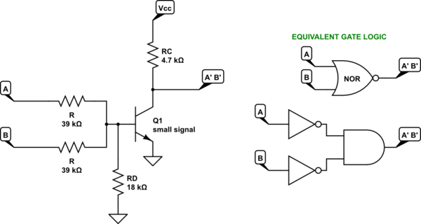
Here is the resulting circuit design:
schematic

simulate this circuit

Given the above, I figure \$V_{TH_{OFF}}\le 480\:\textrm{mV}\$ when both inputs are at \$V_{LO_{MAX}}\$ and that \$V_{TH_{ON}}\ge 720\:\textrm{mV}\$ when one input is at \$V_{HI_{MIN}}\$ and the other is at ground. This should provide enough margin for reasonable operation.

I think you will find that this works well with up to six loads on the output and works over the ranges I've discussed.

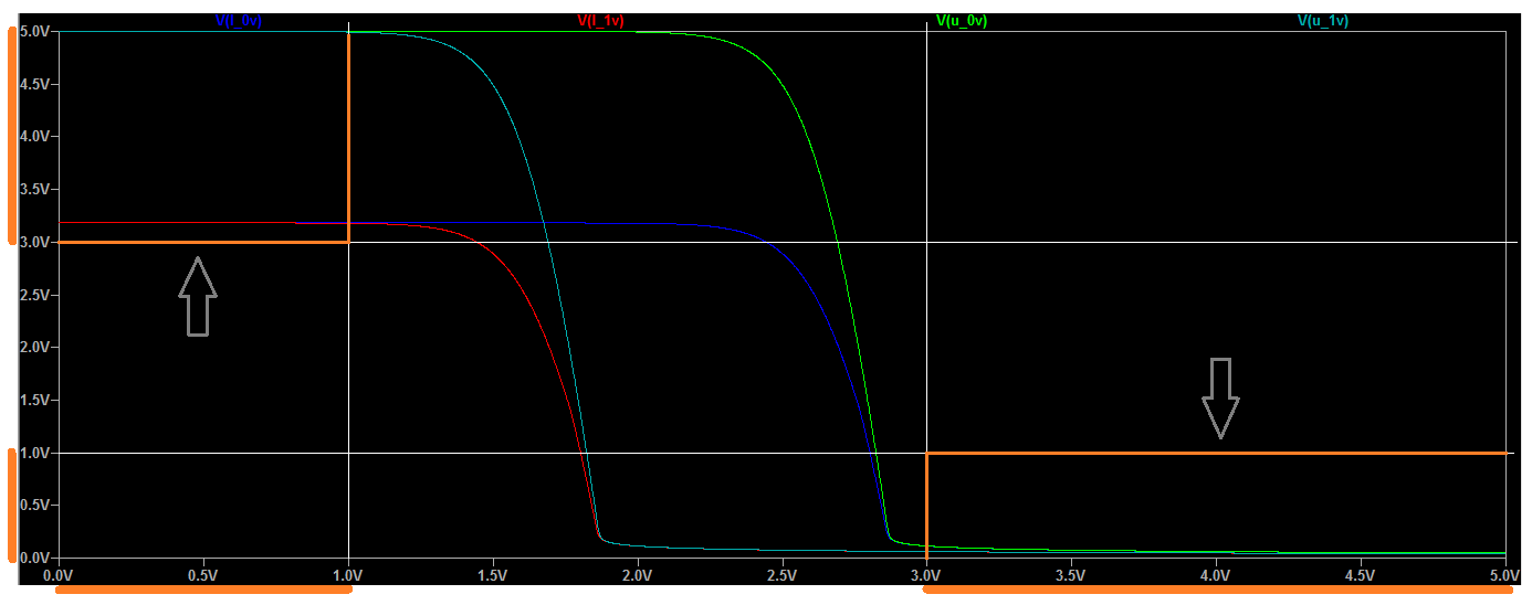
The following image shows four traces covering case (1) and case (2) above, with the output both loaded and unloaded. The x axis is the voltage on the A input, or \$V_A\$. The y axis is the output voltage. The unloaded curves are labeled starting with "U" and the loaded curves are labeled starting with "L". The traces with \$V_B=0\:\textrm{V}\$ are labeled with "0V" and traces with \$V_B=1\:\textrm{V}\$ are labeled with "1V" in their names.
enter image description here


Fuller adder here:

enter image description here

\$\endgroup\$
11
  • \$\begingroup\$ Great answer, thank you! I think I can implement this, but I'm lost on quite a bit of the explanation you gave. Mainly the "pulling down" and "pulling up" voltages is confusing me, though I think it might be a semantic issue. For instance, when you add RD to leak away some of the current to ground and minimize the amount of current through Q1, you say that's "possible collector current pulling down the collector voltage" - what exactly does this mean? Thanks again! \$\endgroup\$
    – Nathan
    Commented Jan 22, 2017 at 2:35
  • \$\begingroup\$ @Nathan The context is that both inputs are LOW, but at the highest design voltage for LOW (1 V.) This will produce a small base current. If the BJT's current gain is enough, it's collector current will be high enough to cause enough of a voltage drop across RC that the collector voltage will be pulled down. This is what I meant by "collector current pulling down the collector voltage." It happens if too much collector current is made possible by too high of a beta. Then even a tiny base current can be a problem and the output will be LOW instead of HIGH, as it should be. \$\endgroup\$
    – jonk
    Commented Jan 22, 2017 at 4:05
  • \$\begingroup\$ Ok, I think I can see this here in this simulator: tinyurl.com/hzzpslo If you tweak the potentiometer up and down I can see Vce drop suddenly at 22k, as you calculated - is this the effect you're referring to with the pulling down of the collector voltage? I suppose this is effectively due to the resistance between the collector and emitter dropping? \$\endgroup\$
    – Nathan
    Commented Jan 22, 2017 at 5:10
  • \$\begingroup\$ @Nathan Yes, that's what I was referencing. A crafted design for production as an RTL family of products would involve still more design work. But this gives a flavor of it. DTL soon took over. Then TTL. Then still better with schottky, and so on since then. But when BJTs were very scarce and resistors very cheap, RTL was the way. (Now BJTs are often cheaper than a cheap resistor and very plentiful. So no one would do it this way, now.) \$\endgroup\$
    – jonk
    Commented Jan 22, 2017 at 5:50
  • \$\begingroup\$ Ok, I understand it now :) I've been able to implement one of my simpler circuits completely in the simulator, so I'm going to try ordering some parts and doing it for real. Thank you for your help! \$\endgroup\$
    – Nathan
    Commented Jan 22, 2017 at 6:18
2
\$\begingroup\$

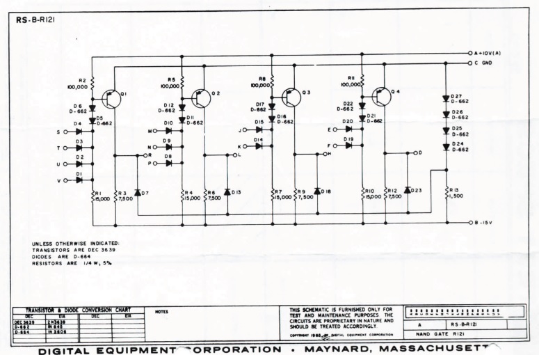
The PDP-8 minicomputer, released in 1965, used DTL (diode-transistor logic) contained on dozens of DEC R-series Flip Chip modules. For example, the R121 card was a set of NAND gates. A list of the R-series cards is shown on this page. Below is the schematic for the R121 card showing the DTL circuits:

enter image description here

Note it used both positive (10v) and negative (-15v) power rails, almost all of the power drawn from the negative supply. This particular card drew 0.4 mA at 10v, and 20 mA at -15v. 0v was considered a logic '1', and -3v a logic '0' and ran at speeds up to 2 MHz.

The schematics for the other cards (inverters, flip-flops etc.) can be found by Googling the R-series card number.

\$\endgroup\$
1
\$\begingroup\$

You need to take a good hard look at the functional equivalent circuits inside basic bipolar logic gates chips. These will show you that to achieve a low impedance output drive for a gate it is necessary to design with a push pull output stage. This is necessary to be able to drive the inputs of more than one or two cascaded gates. Also when this is done the internal resistor values needed to produce the functional gate logic can be made larger to reduce current consumption a lot.

Keep in mind that the usage of bipolar logic chips to build computers and electronics gadgets of yesteryear consumed large amounts of current. It was not uncommon to see systems with 60 or 100 amp power supplies!! As systems got more complex demanding more gates, better technology came along to save the day. First NMOS transistors allowed gates to be built that required virtually no input bias current. That was quickly followed by CMOS which mixed PMOS and NMOS devices together to make logic gates that had few energy wasting resistors inside and lowered idle power by orders of magnitude.

After you experiment around a bit more with your bipolar transistor gates you may want to consider making your building block discrete gates using alternate type components in attempt to duplicate some of the technology that quickly displaced the old logic concepts used on DTL and RTL.

\$\endgroup\$
1
  • \$\begingroup\$ That's really useful, thank you. I hadn't realised just how old RTL is - I suppose it's natural for it to be inefficient. Time to get back to googling, now I have some good keywords :) \$\endgroup\$
    – Nathan
    Commented Jan 19, 2017 at 3:36
1
\$\begingroup\$

Here is a good article about RTL logic: https://en.wikipedia.org/wiki/Resistor%E2%80%93transistor_logic

I recommend reading the section Limitations about fan-in and fan-out as well as noise immunity. If your gates should be modular, the low level of an output should be lower than the threshold of an input to leave some margin for noise immunity and for one output driving one, two or three inputs of other gates. The high level of an output should be higher than the threshold of an input with room for noise immunity and connection of several gates. If you connect several gates in a chain of inverters, the logic levels should not degrade over the chain. A ring oscillator of three, five or seven inverters is a good test, compare the outputs using a two channel scope.

Here are some calcualtions and resistor values: http://www.play-hookey.com/digital_electronics/rtl_gates.html

\$\endgroup\$

Your Answer

By clicking “Post Your Answer”, you agree to our terms of service and acknowledge you have read our privacy policy.

Not the answer you're looking for? Browse other questions tagged or ask your own question.