9
\$\begingroup\$

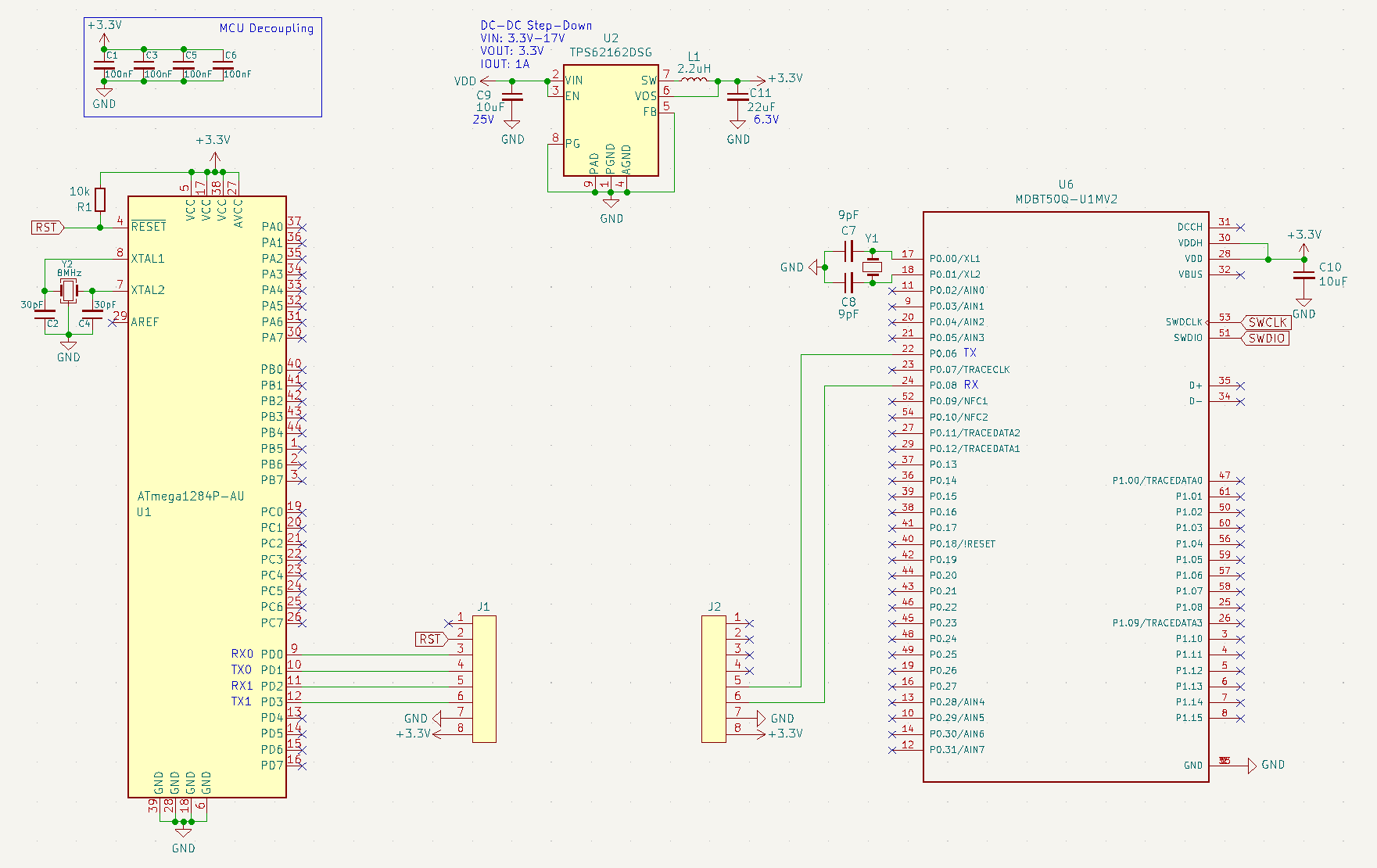
I have devices operating from 2S Li-ion battery (max 8.4V). They consist of 2 PCBs - the first one contains a 3.3V voltage regulator and an ATmega1284P, while the second one has MDBT50Q-U1MV2(nRF52840 based module) on board.

The two PCBs are connected with an 8-pin Pico-Clasp 10cm wire which, among other signals, carries 3.3V, GND, and UART (TX, RX) lines. This is a simplified, stripped-down schematic.

schematic

cable

During normal operation, the nRF module requests a custom status packet over UART (baud rate 57600) every 5 seconds, and the ATmega replies back. Recently, I started experiencing weird issues on some devices where the UART communication stops and does not recover even after device reboot. The firmware on both microcontrollers runs fine without crashing.

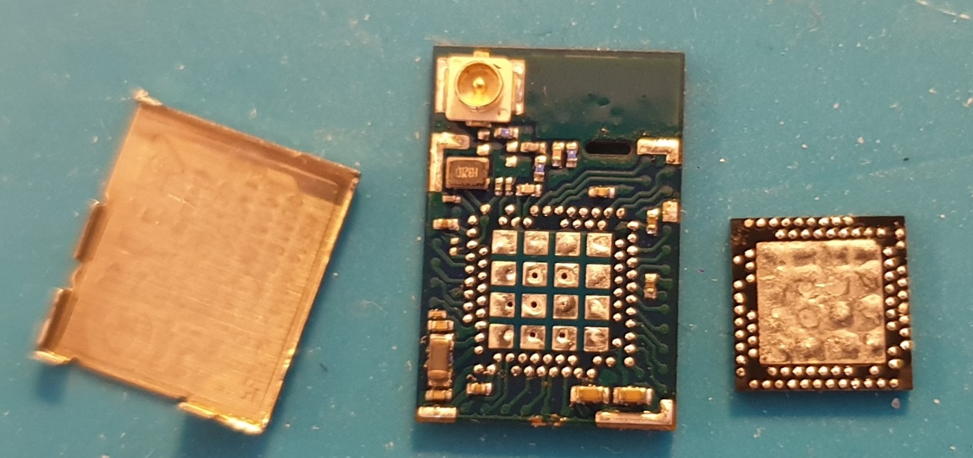
Inspecting the UART lines using an oscilloscope revealed the packets from nRF52840 are still going through, but the logic high voltage level is very small (far from 3.3V). Resistance measurement showed that both GPIOs used for TX and RX on the nRF52840 side have decreased resistance to GND (200ohm instead of 2.5M measured on other devices). To eliminate potential short somewhere in the module, I opened the module, desoldered the nRF IC, and measured with the same result, so the short is in the silicon. The ATmega doesn't have problems and works fine with a different nRF module.

nrf

This sounds to me like a prime example of the internal clamp diodes being fried by ESD, however:

  • the device is encapsulated in an enclosure, so no GPIOs are accessible from outside
  • it's always only the two (RX and TX) pins on the nRF side that are showing this issue
  • every device is fully checked for several days after being assembled and works fine - the problems arise later, while in the enclosure

My questions are:

  1. The enclosure is made of the SLS 3D printed nylon. Could it generate enough static electricity during movement to cause something like this? The devices are experiencing a lot of mechanical movement (repetitive shaking).
  2. Since it's always the UART pins, could it be the ATmega1284P outputting something destructive? It is 5V tolerant but runs on 3.3V so I wouldn't assume it ever exceeds it.
  3. Could any dangerous voltage spikes be induced in the 10cm long wire during rapid movements (e.g. Eddy currents), or impedance mismatch / reflections due to high speed signal and long wires?
  4. The UART lines are connected directly. Would it make sense to include an external ESD protection such as steering Schottky diodes + TVS (e.g., SRDA3.3), maybe series resistor to limit the current. Or even small mosfets, as used in level shifters, just to isolate the domains? What configuration would you recommend, and on which of the PCBs?

I would be really helpful if you could help me figure out what could be causing this issue.

Thank you.

EDIT:

Thank you for your replies.

Just to clarify a few points:

  • The cable is never hot-plugged. Once the device is assembled, it stays connected.
  • As I mentioned, I have provided a simplified, stripped-down schematic, which only includes the shared connections. In reality, the ATmega PCB also contains motor drivers, push-button controller, high-side switch mosfet with voltage divider to sense the battery, buzzer, etc. The nRF board has I2C sensors, IMU, external flash, and one section of the PCB has an analog front-end IC (with separate, filtered 3.3V).

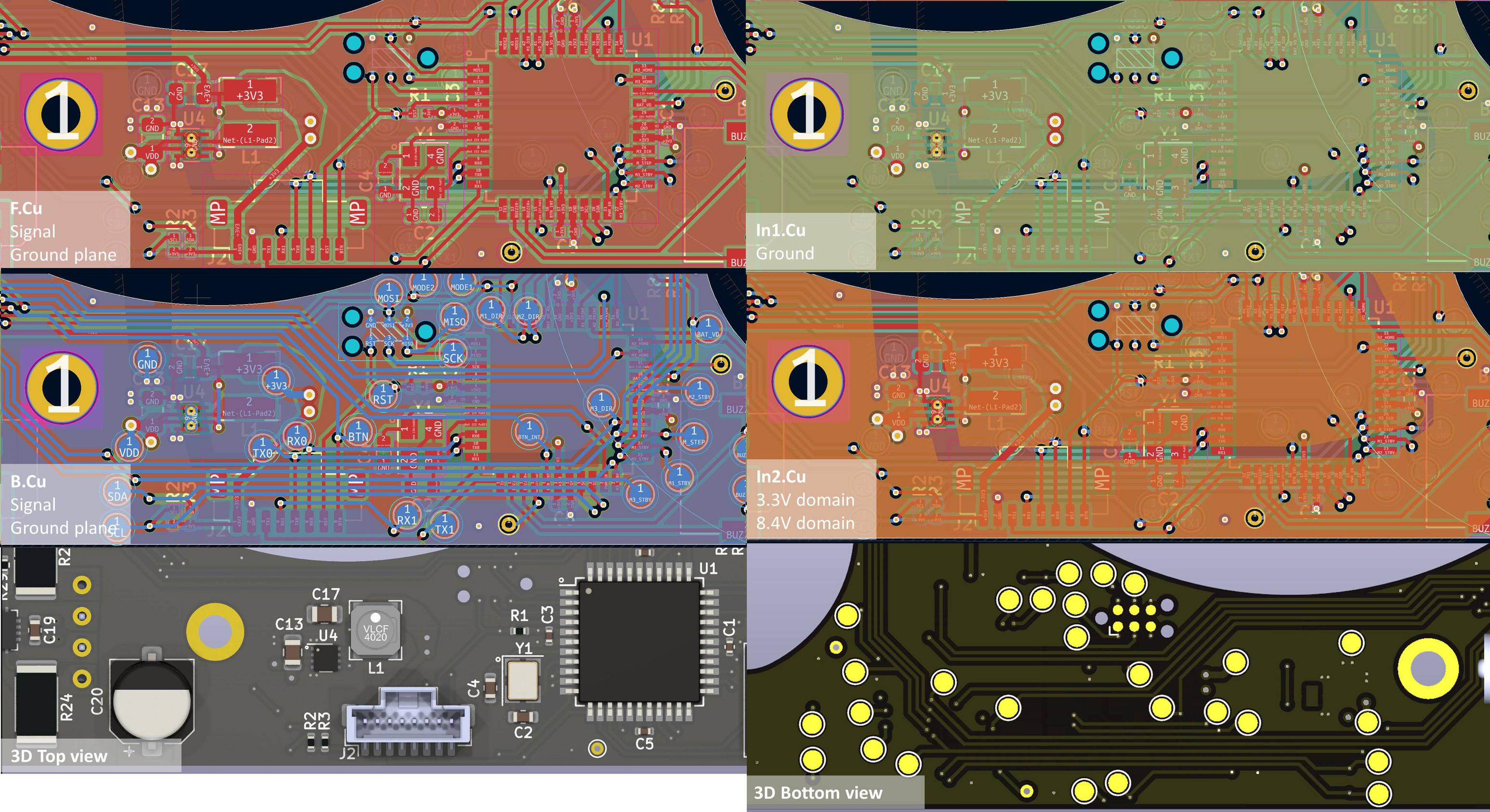
I am attaching a layout views for both PCBs.

PCB1-layout

PCB2-layout

  1. I have noticed that the 8.4V domain runs on the In2.Cu layer around the vias with the UART lines. Is it possible that a momentary short occurs between them, so the nRF (abs. max 3.6V) fries, while the ATmega (abs. max 6V) survives?
  2. I have quite a few test/programming pads on the PCB. Can these serve as ESD pickup points even when the device is fully enclosed?
\$\endgroup\$
2
  • \$\begingroup\$ Please show the layout of both the board that holds the RF module, and the board that holds the MCU and the power buck converter. If those are 2-layer boards, then good pictures or scans of bare board are easier to look at than screenshots from the PCB program. \$\endgroup\$ Commented Apr 5, 2023 at 21:02
  • \$\begingroup\$ Yes, this is a classic case of unshielded cables being susceptible. Therein lies the answer: either filter and clamp the signal lines (and power too; bypassing >1uF is usually enough), or use coax (probably infeasible with the connectors, which will always add some unshielded length). \$\endgroup\$ Commented Apr 6, 2023 at 1:07

3 Answers 3

7
\$\begingroup\$
  1. The enclosure is made of the SLS 3D printed nylon. Could it generate enough static electricity during movement to cause something like this? The devices are experiencing a lot of mechanical movement (repetitive shaking).

It could generate triboelectricity, and it's not a good static shield since it has very low conductivity. So that's a pretty bad choice for an enclosure when ESD is a potential problem.

  1. Since it's always the UART pins, could it be the ATmega1284P outputting something destructive?

No other pins seems to be connected, so I don't quite see why you say "it's always the UART pins". Are any other pins connected to that cable, other than power?

  1. Could any dangerous voltage spikes be induced in the 10cm long wire during rapid movements (e.g. Eddy currents), or impedance mismatch / reflections due to high speed signal and long wires?

These wires are just ESD pickups at this point. There is no conductive shielding of any sort between the wire and external ESD. But ESD may not necessarily be a problem. Just something to keep in mind.

  1. The UART lines are connected directly. Would it make sense to include an external ESD protection such as steering Schottky diodes + TVS (e.g., SRDA3.3), maybe series resistor to limit the current.

Sure, the external ESD protection can't hurt, and the series resistors can't hurt either. Shunt-type protection must be located immediately to the point where the signals enter the RF PCB, i.e. right next to the connector.

I don't like the idea of so few ground wires on that cable harness. I'd add at least 1 ground connection - on pin 1 - and connect it on both ends of the cable.

I'm more concerned that the UART pin damage is a symptom of a different problem, though. I'd add a snubber across the 3.3V/GND at the entrance to the RF board. And perhaps a bit more decoupling capacitance. The RF module is drawing current in spikes whenever the transmitter turns on. Those transients, in connection with the wire inductance, may be overstressing something. Maybe.

Decoupling capacitors must be X7R or a similar low-voltage-coefficient types. Do not use high-K types like Y5V etc. - those turn into tiny capacitors when DC bias is applied to them.

You also seem to be missing a bunch of power connections on the RF module. All GND must be connected: pins 1, 2, 15, 33, 55. You seem to have connected only one of them?!

It may also help to match the decoupling capacitors for U2: C9, C11 to the frequency of the converter. I.e. look carefully at the capacitor datasheets, and select parts that have self-resonant frequency aligned with U2's switching frequency under some steady state. Since U2's frequency is variable, this will not be as effective as it otherwise would be, but still bringing the average U2's operating frequency closer to the capacitor self-resonance would be a good idea. In all cases, capacitor self-resonance should never be lower than U2's frequency. You'll have to characterize U2 to see, in your application, what's the fastest it will switch, across use cases and battery states. And then select capacitors with self-resonant frequency smack at the upper end of that range. This is in the category of potentially evil micro-optimization, and shouldn't be necessary in a design that has good margins, but once you get it working reliably without this tweak, selecting the capacitor SRF as the last step in the design process won't hurt.

\$\endgroup\$
1
  • \$\begingroup\$ Thank you. I have edited my answer to add layout view and clarify a few details. \$\endgroup\$
    – st4n13y
    Commented Apr 6, 2023 at 9:47
4
\$\begingroup\$

While it's impossible to prove a negative, I don't think this is an ESD problem. I would suspect one of the two culprits:

  • SW bug which results in pin misconfiguration. It could be that pins on both sides are configured as outputs, perhaps just for a short time during startup sequence. It may be not enough to damage the pin during your test run, but repetitive high current eventually results in damage.

  • Poor connections between the PCBs and the cable, especially the GND pin. If the GND pin becomes disconnected, then the entire current consumed by the nRF52840 has no other way but the TX/RX pins. Again, the connectors may be good enough to pass your test, but will fail in the environment due to vibration.

One "palliative" solution could be to add 1k series resistors on the TX/RX lines. If your baudrate is high enough so that rise/fall times with 1k resistors are a problem, you can add ~100pF capacitors in series with the 1k resistors. Resistors will limit the current to <3.3 mA per pin, no matter how the SW configures them and how good your GND connection is.

A real solution would be to find out which is the true cause and fix it. Perhaps it's the stray GND issue, in which case running the GND via both pin 1 and pin 8 of the cable will help. This configuration would ensure that GND is the first line to make contact (or the last line to lose contact) even if the connector becomes tilted sideways.

PS. I understand you have two separate +3.3V / GND nets connected by the jumper cable. It would be better if you named them differently, e.g. VCC_MCU and VCC_NRF. As it looks now, all devices will stay powered if the cable is removed, which I suspect is not the case.

\$\endgroup\$
4
\$\begingroup\$

I like all of "Kuba hasn't forgotton Monica's" answers, but I am worried that your problem is likely just load regulation of the power supply switching circuit. Unless you are doing something else with your +3.3V, the switching device you have chosen feels like it is going to have some load regulation issues with loads this small. The nRF device "absolute maximum ratings" are pretty tight, and if the voltage gets to 3.6 volts, an internal LDO regulator takes over and the absolute maximum ratings for VinH do not continue to go up with increasing Vdd. The ATMEGA's VoutH is dependent on the supply voltage, and continues to increase with Vdd.

The good news is that the internal voltage regulators are available as an output pin on the nRF device. I would put in an opto-coupler or similar isolation IC and power the nRF side from the device's internal voltage regulator. That way you would be protected from overvoltage on the VDD knocking out your only two connected pins. You "might" get away with putting resistors in series, but the isolation circuit is a surer bet.

From nRF Absolute Maximum Ratings:

enter image description here

Once the supply voltage gets above 3.6 volts, any voltage above 3.9 volts on RX will damage the nRF device. So if your supply voltage goes up for any reason, the output voltage from the ATMEGA IO will increase, and you will have the exact symptom you are seeing.

\$\endgroup\$
6
  • \$\begingroup\$ Oh, another idea along these lines -- if the cable was ever hot-plugged i.e. one side powered on and the cable plugged in, the inrush transient can up to double the supply voltage momentarily. \$\endgroup\$ Commented Apr 6, 2023 at 7:51
  • 1
    \$\begingroup\$ If I run the nRF in DC/DC or LDO mode, it expects 3.6V - 5.5V which is both, above the nominal output of my regulator, and below the battery supply voltage. \$\endgroup\$
    – st4n13y
    Commented Apr 6, 2023 at 9:41
  • \$\begingroup\$ Please see the edit in my answer. At this low current load, your power supply voltage could increase from load regulation, or just from an external device input that pulls up the supply. \$\endgroup\$ Commented Apr 6, 2023 at 13:56
  • \$\begingroup\$ I have edited my post to clarify that the device consists of more components, so the average power consumption is always around 80mW. Also, the load regulation (Figure 18) and output voltage ripple (Figure 22) specifications in the datasheet (ti.com/lit/ds/symlink/tps62162.pdf) do not indicate that this would even be an issue. Please, help me understand if you mean something else. \$\endgroup\$
    – st4n13y
    Commented Apr 6, 2023 at 18:16
  • \$\begingroup\$ You're probably OK with the TI device if you are always around 80mA. The concern is if you are running with a load and you suddenly drop it. The ATmega device draws a few milliamps, depending on the frequency. Any external device with a higher voltage attached to its input will pull its internal supply up; we have trouble getting these things to go into reset on power down if there is any powered device connected. \$\endgroup\$ Commented Apr 6, 2023 at 19:08

Your Answer

By clicking “Post Your Answer”, you agree to our terms of service and acknowledge you have read our privacy policy.

Not the answer you're looking for? Browse other questions tagged or ask your own question.