I am currently building a soft latch circuit in a CAD editor.
I want to use a PNP transistor, and have 2 choices for this component.
However, I am confused when comparing the datasheets of the components with the symbols and footprints in the CAD editor.
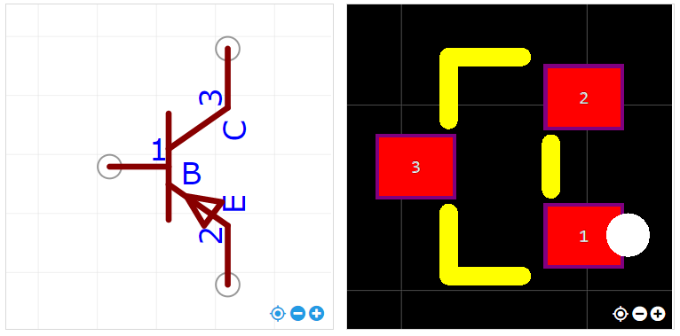
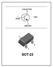
Part 1 looks like this. Pin 1 is base, pin 2 is emitter, pin 3 is collector. This lines up with it's data sheet. Also the footprint numbering lines up with the datasheet.

(Screenshot from EasyEDA)
(Image source: LCSC - Galaxy Microelectronics MMBT3904 datasheet)
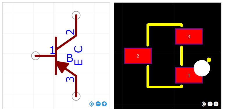
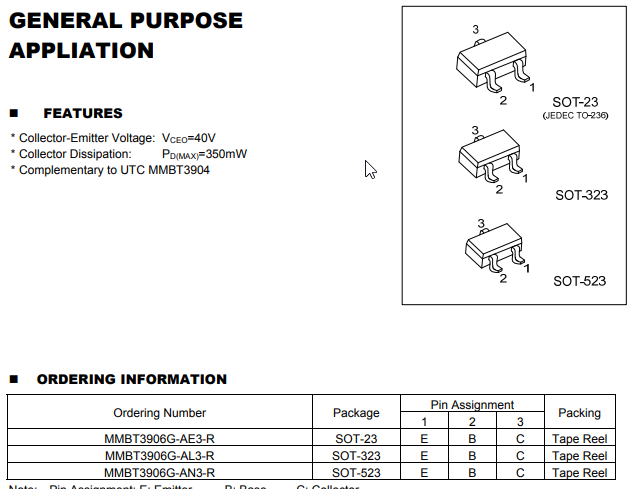
For part 2, Pin 1 is base, pin 2 is collector, pin 3 is emitter in the CAD symbol. Ok, I understand that the pin numbering could be different. Looking at the datasheet, however, pin 1 should be emitter, pin 2 should be base, and pin 3 should be collector. Also, the footprint pin numbering is different then in the datasheet.
I tried to replace the symbol of part 1 in my schematic with part 2, but now I find out that the pins are swapped. Is it true that I can never just replace symbols in the schematic for transistors?

(Screenshot from EasyEDA)
(Image source: LCSC - Unisonic Technologies MMBT3906 datasheet)
I saw in a video that PNP/NPN transistor symbols are not unified. Does the empty/filled arrow in the symbol represent something different? Is the symbol and footprint for the second part plain wrong? Should I trust the datasheet of the second part, or not use it at all?


