The datasheet is very sparse, but all the information you need is plainly on it.

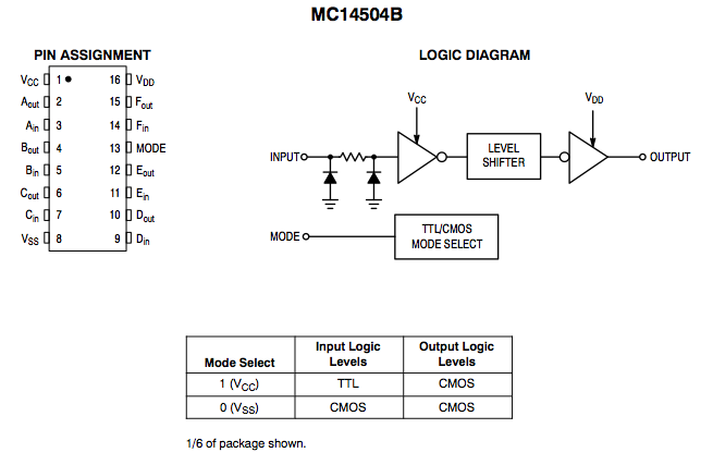
What you see here is a internal description of how it works, and the Mode Select pin. This is a 6 input to 6 output level shifter. It is not bi-directional, and you can only translate from one level to the other, no mixing and matching. The diagram shows that an input goes into the inverter (not gate), powered by VCC. It is then shifted before going into another inverter, powered by VDD, resulting in the output.
From this you can see that Vcc is the Voltage Supply for the Input level, and VDD is the Voltage Supply for the Output level.
The Mode select table tells you how the Mode pin should be handled. The TTL and Cmos does not refer to simply voltage levels, but how to interpret them.
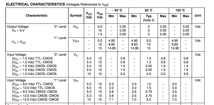
And the Electrical Characteristics tell you the rest.

Here you can see what voltage, comparatively, will be interpreted. Cmos treats a Low and a High roughly equally. A Input Low (0) is treated as a little under half of the Voltage Supply level (Vcc), and a Input High (1) is treated as a little over half of the Vcc (When VCC = 5, anything under 1.5V, then up to 2.25v is logic 0, anything above 3.5V, then until 2.75V is logic 1).
TTL on the other hand, has a smaller, fixed range for logic low. An input (at VCC = 5v) between 1.5 and below is Logic 0, and 1.5 and above is Logic 1.
You need to look at the STM32's datasheet to figure out if it uses TTL or cmos level output.


