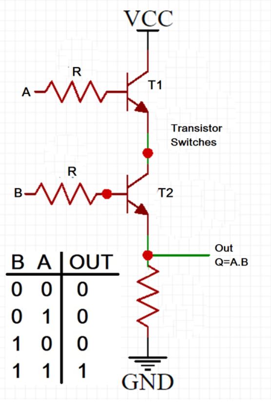
Edit: Before you read on, the ideas I present here are not optimal. There are probably common-base solutions that better fit the requirement for AND behaviour, and you could probably pare down a classic TTL design from inside a 74 series logic IC for better results.
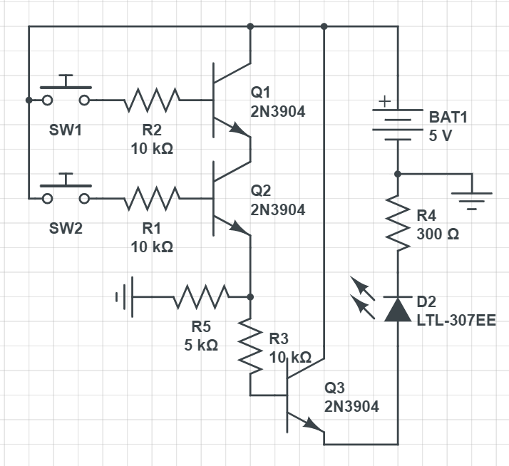
If you are going to chain several such "modules" together, then you require voltage gain. As you have it, all your transistors are connected "common collector", otherwise known as "emitter follower". As the name suggests, emitter potential follows the base, with a voltage gain of 1, and a base-emitter-junction-voltage of \$V_{BE}=0.6V\$ lower.
See this answer for information about followers. It references source followers, using MOSFETs, but the principle is the same for BJTs.
In your circuit, output potential at the collector of Q3 can never be higher than \$5V - 2\times V_{BE} = 3.8V\$, because you incur a loss of \$V_{BE}\$ at Q2's emitter, and another \$V_{BE}\$ at Q3's emitter. Imagine such losses accumulating with each cascaded logic stage. After two or three stages, there's nothing left.
Ideally you would want the output of any such logic gate to be a clear, emphatic +5V or 0V, so you will probably require voltage gain greater than 1, to bring the signal back to that maximum potential swing. Using a single transistor to achieve this would necessitate one of the following common emitter (as opposed to common collector, or emitter follower) configurations:

simulate this circuit – Schematic created using CircuitLab
On the left we use an NPN device, on the right is PNP. Note that I haven't included base resistors, to limit base current, because whether you need them depends on the source of signal driving the bases. As you should be aware, this configuration inverts. A high base potential will cause a low output (collector) potential, and vice versa.
Your choice of NPN or PNP here depends on what your output is intended to drive (whether the following stage or module is sinking or sourcing current), and also (to some extent) whether the previous stage is a source or sink of current.
I am not suggesting that you must use these configurations, I want simply to point out that at some point in the chain, you will probably have to recover any "lost" signal amplitude, with some voltage gain above 1, and this is a way to do that. Just be aware of the inversion that also occurs.
You are correct in your assessment that the base-emitter junction of Q2 is acting like a diode, causing a high potential at its base to raise emitter potential, in spite of whatever Q1 is trying to do. Q1 is powerless to prevent this.
MOSFETs do not suffer this problem, since their gates are completely isolated from drain and source; no such "diode" junction is present between gate and source to cause this behaviour. That's why it's OK to use MOSFETs in this configuration, but not BJTs. If you swap Q1 and Q2 for MOSFETs, then your problem goes away, although you'll need extra resistors to set explicitly gate potential while the switches are open, and you'll have to contend with a much larger voltage drop of \$V_{GS(TH)}\$. Such "source follower" arrangements would work better with a larger supply, say +12V instead of +5V.
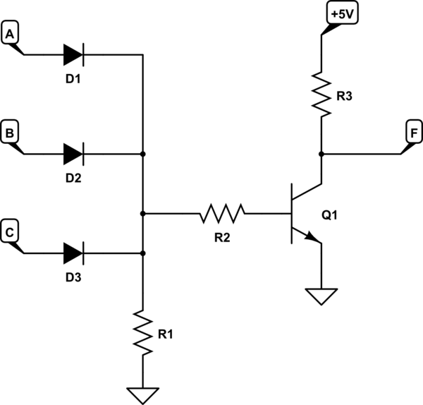
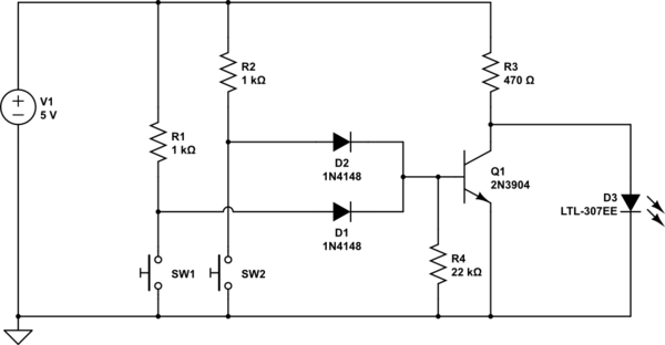
I'll assume from here on that you wish to stick with bipolar junction transistors. Actually, let's start with using just diodes. Here are a couple of interesting setups called "Diode-OR" (left) and "Diode-AND" (right):

simulate this circuit
On the left, any high input at A, B or C will forward bias the corresponding diode, causing it to conduct, and "pulling" up the potential at F. This is the behaviour you expect from an OR gate.
On the right, the output is high (pulled up by R2), unless any of the inputs A, B or C are low, in which case the corresponding diode is forward biased, highly conductive, and "pulling down" the potential at F. That's the behaviour of an AND gate.
You can create any logical gate function using only what I've shown above, by performing boolean manipulations of your desired function to be in terms of NOT, AND and OR. For example, NOR:

simulate this circuit
Your question about how to make an AND gate is already answered, then, using just diodes, but it doesn't amplify, and there's still a diode-junction "loss" of 0.6V which may be problematic for subsequent stages.
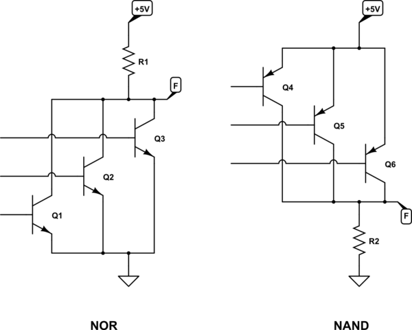
One of the coolest things you can do with common-emitter configurations is combine several, and connect all the collectors together:

simulate this circuit
On the left, any "on" transistor (base high) pulls F low, which is a NOR function. To the right, by using PNP transistors we have a similar condition in which any "on" device (base low) will take the output F high, for NAND behaviour.
This arrangement is used very often with "open-collector" outputs. Check out the LM393 comparator, and the 74HC03 logic IC. These have open-collector or open-drain outputs that can be wired together in this way (a technique called "wire-OR" or "wire-AND") to combine outputs from multiple devices without the need for additional logic gates.
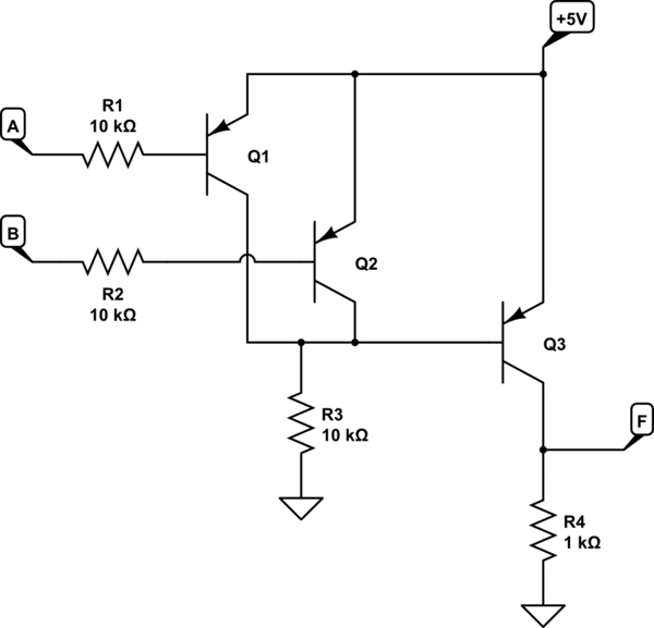
By inverting the output from the right hand circuit, we have AND, which yields my second suggested solution to your problem:

simulate this circuit
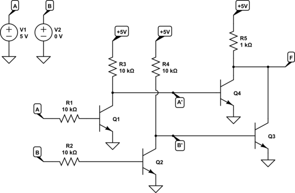
Finally, if you insist on using NPN transistors to perform AND, one way is to invert the inputs, and then NOR them:
$$ A \cdot B = \overline{\overline{A} + \overline{B}} $$
This is my third solution to your problem:

simulate this circuit
A couple of points about this last design. The nodes A' and B' do not ever rise above +0.7V, since they are clamped to this maximum by the base-emitter junctions of Q3 and Q4. The reason I can get away with so few resistors in this design is due to the fact that R3 and R4 form not only part of the inverters, but also serve as current-limiting base resistors for Q3 and Q4. This is what I alluded to earlier - whether you choose PNP or NPN devices depends on what comes next, and what comes before. In this case I got lucky, and was able to fulfill two goals with a single resistor.
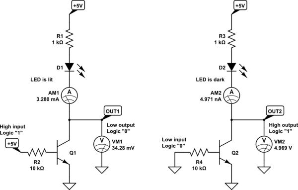
Lastly I want to warn you about confusing an LED being on (a load passing current) and a logical "high":

simulate this circuit
Here I demonstrate that the LED will be lit when the output is low, not high! That's somewhat counter-intuitive, and a big source of confusion. In all my examples above I have treated high and low potentials and corresponding to logic 1 and 0 respectively, and if you build any of those circuits with LEDs to indicate logic state, beware this potential gotcha!
Update
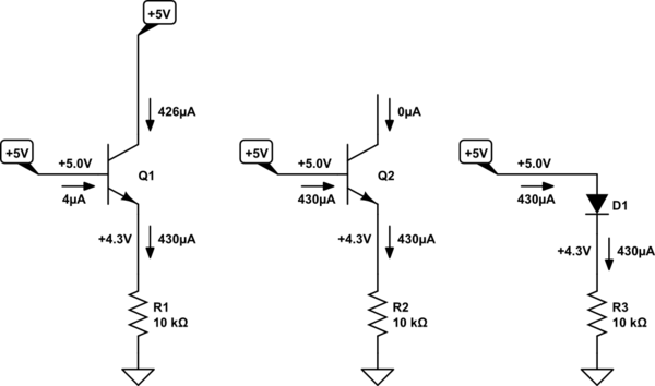
To address you comment, and clarify the follower behaviour of your Q2, consider this:

simulate this circuit
On the left is a normal emitter follower. The base is held at +5V, and this places the emitter 0.7V below that, at +4.3V. Due to the "load" R1 at the emitter, by Ohm's law we can say that the current through R1 is 430μA.
Pay attention to where that "emitter current" is coming from. If the collector is connected to +5V, almost all the current comes in via that route, and the base only contributes only a tiny amount in comparison. The transistor is operating as you would expect, as a current amplifier, in which the source of +5V at the base is required to supply very little current, and the transistor takes care of the rest, drawing current from whatever supply is connected to the collector.
What happens, though, if you don't connect a power source to the collector? That's exemplified in the middle circuit. At first it doesn't seem that much changes, since the emitter is still at +4.3V, the same as before, and the current through the load is 430μA, also the same as before. The difference is where that current comes from. With no power supply at the collector to source any current from, it's the source at the base which has to do all the work. All 430μA comes in via the base instead.
The reason for the emitter rising to +4.3V in this case is the base-emittter junction, which behaves like any P-N junction (AKA diode) behaves. When forward biased (as it is in the middle circuit), it develops 0.7V across it, and conducts heavily.
To illustrate this, I've reproduced the same conditions on the right, using just a diode instead of the transistor. From the perspective of load R3, conditions are identical. The center and right-hand circuits above are electrically equivalent.
Focusing on the left and middle circuits, the only difference is the presence/absence of a connection to +5V at the collector. If you imagine that this connection/disconnection is under control of another transistor (Q1 in your original circuit), its state (on or off) cannot possibly have any effect on the potential across our load. All it can change is the route via which those 430μA are sourced, but the load will still have 4.3V across it, regardless.
That "diode" between Q1's base and emitter makes it impossible to use two or more bipolar transistors, as you've configured them, to behave like on/off switches in series, as you had hoped.


