0
\$\begingroup\$

I want to make a PCB for DC-DC converter. I used TI’s Webench tool to create a buck converter design using the TPS5604 IC. enter image description here
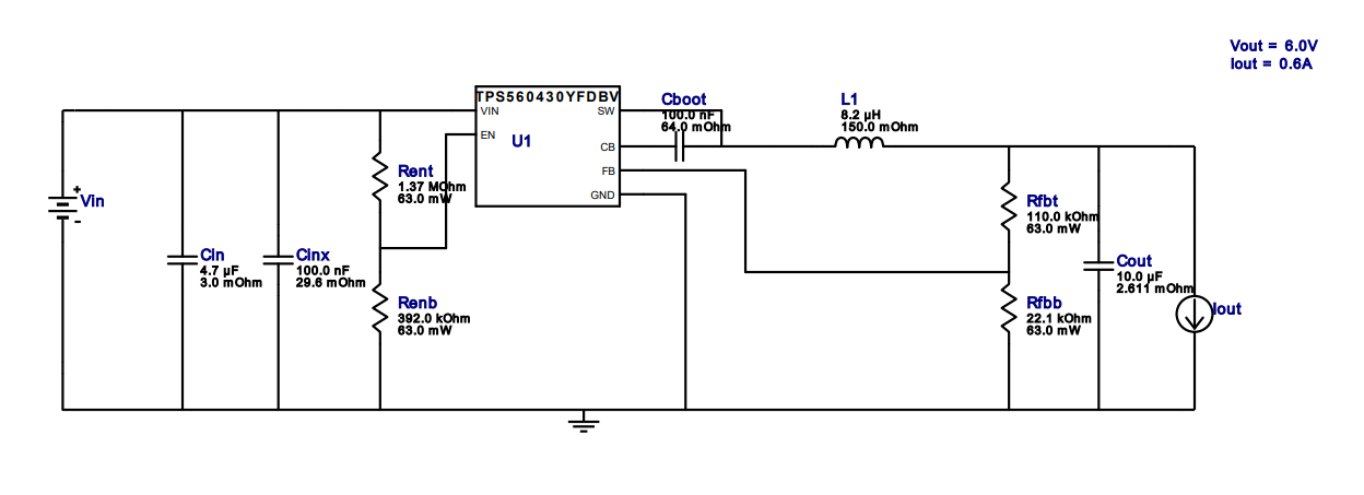
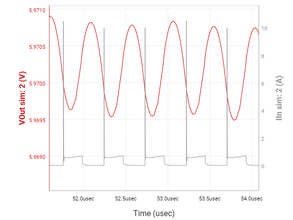
The input voltage is 13.5V and output voltage is 6V and maximum current is 600mA. The problem is according to the Webench simulation the input current reaches 10A at the start of each switch cycle. I understand that at the start the input current will reach higher currents (around 5A). But why does it rise to such high currents in steady-state?

enter image description here

\$\endgroup\$
4
  • \$\begingroup\$ 150mohm resistance at 8.2uH is a terrible inductor. Try better one. \$\endgroup\$ Commented Jun 9, 2023 at 14:55
  • 1
    \$\begingroup\$ I used 18u 100mOhm inductor. Nothing chanegd. I don't think the spike is related to inductor because it doesn't occur at output. It occurs at input. \$\endgroup\$ Commented Jun 9, 2023 at 15:10
  • \$\begingroup\$ The inductor resists changes in current. No, this spike is capacitive, related to the high side FET turning on (and the voltage at the SW node changing from 0V to 12V very quickly). In less integrated designs, it is common to put resistors on the gate drivers and the boot pin to soften these transitions. \$\endgroup\$
    – Troutdog
    Commented Jun 9, 2023 at 15:34
  • \$\begingroup\$ Try ideal inductor (no resistance) if something changed. \$\endgroup\$ Commented Jun 9, 2023 at 16:02

2 Answers 2

3
\$\begingroup\$

I don't know the particulars of Webench but it would seem their TPS560430 model is timed incorrectly, giving shoot-through.

Or the model is actually correct to the real part, and it really is that bad. Who knows. I haven't used it myself.

In any case, the peak is related to the device, not the components around it. It can be ignored for purposes of selecting other components. It will affect overall efficiency, at least to the extent the simulated efficiency is representative.

\$\endgroup\$
3
  • \$\begingroup\$ Most likely. Note though, that when the top FET turns on, it will have to charge the bottom switch's outputs capacitance. So there is an inevitable brief (capacitive) shootthrough by design in Buck regulators. \$\endgroup\$
    – tobalt
    Commented Jun 9, 2023 at 17:39
  • \$\begingroup\$ Indeed. I have even seen regulators, and controllers, where the dead time is set such that the low side body diode is forward-biased for some 10s of ns, which happened to be less than the transit time of the junction thus activating a much sharper or even step-recovery phenomena, greatly increasing emissions. Obviously, integrated regulators offer even less control over this timing than controllers do, so you're pretty much stuck with whatever it does; your only recourse is to try a different regulator. \$\endgroup\$ Commented Jun 9, 2023 at 17:43
  • \$\begingroup\$ I will go ahead and build the circuit. Then we will see if the problem is with the model or the real part. \$\endgroup\$ Commented Jun 12, 2023 at 14:46
0
\$\begingroup\$

When the top FET turns on, it will have to charge the bottom switch's output capacitance. So there is an inevitable brief (capacitive) shootthrough by design in Buck regulators.

This large current spike therefore occurs in all buck regulators to some extent.

In Buck regulators, the input capacitance's loop inductance is very critical anyway. Minimizing it and using MLCCs as the input capacitor will allow this current spike to be drawn without much voltage drop on the supply.

\$\endgroup\$

Your Answer

By clicking “Post Your Answer”, you agree to our terms of service and acknowledge you have read our privacy policy.

Not the answer you're looking for? Browse other questions tagged or ask your own question.