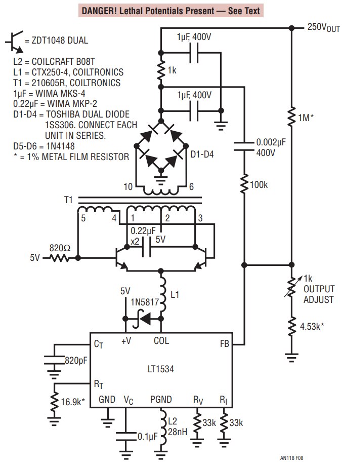
The RC adds a zero to the control loop, and also samples from earlier in the output filter (the first capacitor, at the rectifier), which (somewhat) avoids the pole from the following RC.
The exact details of the control loop may not be obvious. The oscillator circuit[1] acts as a dominant pole, more or less, but may be a complex pole pair, depending on the supply inductance and other control details.
To explain how, while stopping short of a proper proof: model the inverter as a mixer. It switches synchronously with the resonant frequency, so any modulation around Fo (say, amplitude or phase change) is reflected directly as resistance or reactance at the supply port. Basically, the dominant pole will be the tank acting as twice the resonant capacitance (0.22µF in the diagram) (or I suppose it's more, due to the center tap; I'd have to work it out to see what the exact ratio is), in series with the supply inductor (L1 in the diagram). So, the inverter overall, with respect to the DC port, has an equivalent L+(R||C) characteristic. Of course, which element is dominant (R or C), depends on the load condition. Hence, dominant-pole (single real pole, LR character) to resonant (damped LC).
There is some additional effect of the supply inductor, because it acts in parallel with alternate halves of the winding, having a [2nd] harmonic or parametric effect. The ideal (read: simplest) case is with a relatively large inductor (so that its current ripple is small), or alternately for a current source while ignoring AC voltage on the center tap (or rather, taking the average over a full cycle). Smaller values will distort the waveform and you may want to simulate it to see the overall effect (or maybe it's not so bad to analyze as well, I'm not sure).
"Pole" and "zero" are... rather abstract, but precise terms.
While this is officially an EE-design Stack, many readers may not be majors/graduates who have understood the definitions of these terms before, so it probably bears explaining here.
The abstraction is as so:
- Consider the transfer function of a lumped-element filter (that is, a two-port network of RLC components).
- The transfer function can be expressed as the ratio of two polynomials. The order of which are given by the number of reactive (L or C) components, and the topology.
- Factorize the polynomials. Factors of the numerator are called "zeroes", and factors of the denominator are called "poles".
In simplest terms, a "pole"/"zero" is a frequency, around which, the gain vs. frequency of the transfer function changes. How fast, and by how much change, depends on the distribution of poles and zeroes near that point.
Of particular importance to control theory, poles and zeroes dictate how fast and precisely a control loop can respond. The limiting case is determined by gain and phase margin. Poles generally dominate the "slowness" of a system's response. Zeroes can potentially cancel out poles, improving response; but zeroes can also introduce excess phase shift (a non-minimum-phase system), reducing stability and bandwidth.
Other notes:
It's peculiar that these are labeled "Royer", when they are clearly Baxandall oscillators. I don't know whether Jim Williams* was aware of this; or knew and didn't care, or chose to write this anyway because it was the generally more familiar term at the time. (The most common abuse of this term today, seems to be the "ZVS driver" circuit which shows up often in Tesla coil and induction heating circles.)
[1] To be clear, "Royer" means a square-wave converter in which commutation is driven by magnetic saturation of the feedback transformer (which may also be the main/output transformer). The current-sourced (or inductor-supplied) resonant transistor oscillator was first investigated by Baxandall (of audio tone control fame).
D5/D6 in Fig.1 (diode-strapped 2N4393 JFETs) are only used for, I think, transient protection, in particular to account for output short-circuit conditions. They don't need to be such low-leakage diodes (which is a classic application of JFETs, as low-leakage diodes); but, how much leakage is tolerable, depends on how precise the output needs to be. (Evidently not very much, considering the adjustable resistor in circuit!)
Q1 in Fig.1 (common-source MOSFET) feeds an inductor, which doesn't seem to do very much: the drain output characteristic is current-sourcing already. Given the large series gate resistor (10k), the intent was probably to allow Miller effect to reduce its output impedance at the oscillation frequency and/or harmonics. But without damping (an R+C across the transistor, perhaps), it might ring or oscillate at some frequency. If the gate were driven from a lower impedance source, and source degeneration resistance was added (or even a BJT used, which can have lower capacitance than an equivalent MOSFET), the inductor value can be greatly reduced, perhaps omitted entirely.
*No relation, but it's a fun coincidence, eh?

