2
\$\begingroup\$

I want to build a circuit with the following design:

  • 3 inputs
  • 1 NOT gate
  • 2 AND gates
  • 1 OR gate

This is my truth table:

 I1 | I2 | I3 || output

 0  | 0  |  0 ||   0       
 0  | 0  |  1 ||   0       
 0  | 1  |  0 ||   1       
 0  | 1  |  1 ||   1       
 1  | 0  |  0 ||   0       
 1  | 0  |  1 ||   1       
 1  | 1  |  0 ||   0       
 1  | 1  |  1 ||   1       

Can someone help me with what components should I buy?

I know there are chips that have AND/OR/NOT gates, but I was wondering if there's a single one that have all of the ones I need - if not, then what should I use specifically?

\$\endgroup\$
4
  • 1
    \$\begingroup\$ Any reason it has to be those particular gates? For example a package with with four NOR gates could be used to make the logical equivalent of the NOT gate and the OR gate. \$\endgroup\$
    – PeterJ
    Commented Apr 30, 2013 at 10:28
  • 5
    \$\begingroup\$ Despite the mention of buying components, this sounds somewhat like a homework question. While homework questions are not expressly forbidden, you are more likely to get favorable response and perhaps answers, if you explain in your question what you have figured out so far and what you are stuck at. \$\endgroup\$ Commented Apr 30, 2013 at 10:30
  • \$\begingroup\$ @AnindoGhosh I couldn't resist trying a Karnaugh map in MathJax ... \$\endgroup\$
    – jippie
    Commented Apr 30, 2013 at 11:16
  • \$\begingroup\$ Wow. Thanks guys I got my answer. Don't worry it's not homework :). I mentioned these gates because I used Karnaugh map, but it is not mandatory - sorry for misleading. Thanks again! \$\endgroup\$ Commented Apr 30, 2013 at 17:00

3 Answers 3

7
\$\begingroup\$

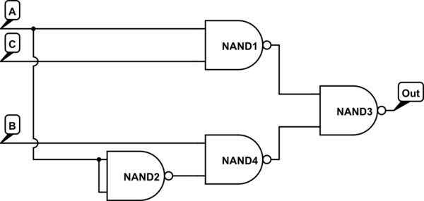
Same deal as Keelan's answer, but using a single 74xx00 series NAND chip (4 gates):

schematic

simulate this circuit – Schematic created using CircuitLab

\$\endgroup\$
5
\$\begingroup\$

First step is filling a Karnaugh map. The first one for little bit help filling the map:

$$ \begin{array}{c|c|c|c|c|} \text{I1}\cdot\text{I2}\cdot\text{I3} & \text{I1}\cdot\text{I2} & \overline{\text{I1}}\cdot\text{I2} & \overline{\text{I1}}\cdot\overline{\text{I2}} & \text{I1}\cdot\overline{\text{I2}} \\ \hline \text{I3} & 111 & 011 & 001 & 101 \\ \hline \overline{\text{I3}} & 110 & 010 & 000 & 100 \\ \hline \end{array} $$

Then fill the truth table $$ \begin{array}{c|c|c|c|c|} & \text{I1}\cdot\text{I2} & \overline{\text{I1}}\cdot\text{I2} & \overline{\text{I1}}\cdot\overline{\text{I2}} & \text{I1}\cdot\overline{\text{I2}} \\ \hline \text{I3} & 1 & 1 & 0 & 1 \\ \hline \overline{\text{I3}} & 0 & 1 & 0 & 0 \\ \hline \end{array} $$

And solve: \$ \text{output} = \boxed{\text{I1}\cdot\text{I3}+\overline{\text{I1}}\cdot\text{I2}} \$

From here follow one of the implementations in the other answers.

\$\endgroup\$
3
\$\begingroup\$

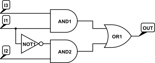
Your output follows this formula:

output = (I1 & I3) | (!I1 & I2)

A circuit would look like:

schematic

simulate this circuit – Schematic created using CircuitLab

For logic gates, you can use the 7400 series:

  • AND: 7408, e.g.
  • OR: 7432, e.g.
  • NOT: 74LS04, e.g.
\$\endgroup\$
2
  • \$\begingroup\$ Not bad : for bonus points, you can redraw it using four 2-input NAND gates, i.e. a 7400. \$\endgroup\$
    – user16324
    Commented Apr 30, 2013 at 10:57
  • \$\begingroup\$ @BrianDrummond I sticked to the parts mentioned by the OP and didn't think of it any further :) I see Bitrex now added your suggestion as an answer so thanks, but I won't add it. \$\endgroup\$
    – user17592
    Commented Apr 30, 2013 at 11:19

Your Answer

By clicking “Post Your Answer”, you agree to our terms of service and acknowledge you have read our privacy policy.

Not the answer you're looking for? Browse other questions tagged or ask your own question.