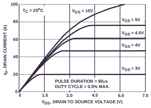
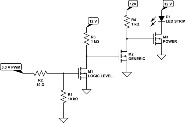
The MOSFET RFP30N06LE you mentioned has \$V_{GS(TH)} < 2V\$, and can be interfaced with the 3.3V digital signal (almost) directly. Even though the datasheet may not explicitly specify \$R_{DS(ON)}\$, you can infer it from graphs of \$V_{DS}\$ vs. \$I_D\$. From the RFP30N06LE datasheet, figure 7 tells you what you need to know:

While these graphs are only typical behaviour (not worst case), they are good enough to show that if you intend to pass, say, 2A of current through your LEDs, \$V_{DS}\$ is well under 0.5V, probably closer to 0.1V. This implies a power dissipation in the MOSFET of \$0.1V \times 2A = 200mW\$ which will barely heat it at all, but you should be aware that the chief cause of increasing \$R_{DS(ON)}\$ is temperature.
For this reason, with a constant current load, you may experience thermal runaway, and should ensure that the device is operating in its "DC Safe Operating Area" shown in figure 4. Of course, a heatsink can always help.
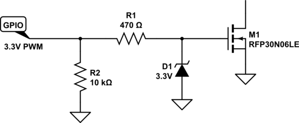
You can do this:

simulate this circuit – Schematic created using CircuitLab
R1 is chosen to limit gate current while charging and discharging gate capacitance, keeping it under the maximum available from the MCU output. Here that current won't be more than about \$I_G=\frac{3.3V}{470\Omega} = 7mA\$. Choose R1 to suit your MCU's output current capability, according to \$R_1 = \frac{3.3V}{I_{MAX}}\$.
With R1 in place, switching speed is somewhat diminished, and miller effects will also slow down switching. At a guess I'd say you're looking at a couple of microseconds for the MOSFET to switch on and off. For lighting PWM that's probably fine, but if it's not fast enough, then you'll probably need a proper gate driver. Your own circuit is not appropriate, as I'll address below.
R1 also provides some protection for the microcontroller against miller effects, which could conceivably raise gate potential beyond +3.3V (or below 0V), but for extra protection I recommend D1. It keeps gate potential within reasonable bounds, and provides an alternative path for miller current other than the fragile MCU output.
R2 keeps MOSFET M1 (and its load) switched off while the MCU output is high impedance, prior to being configured as a PWM output.
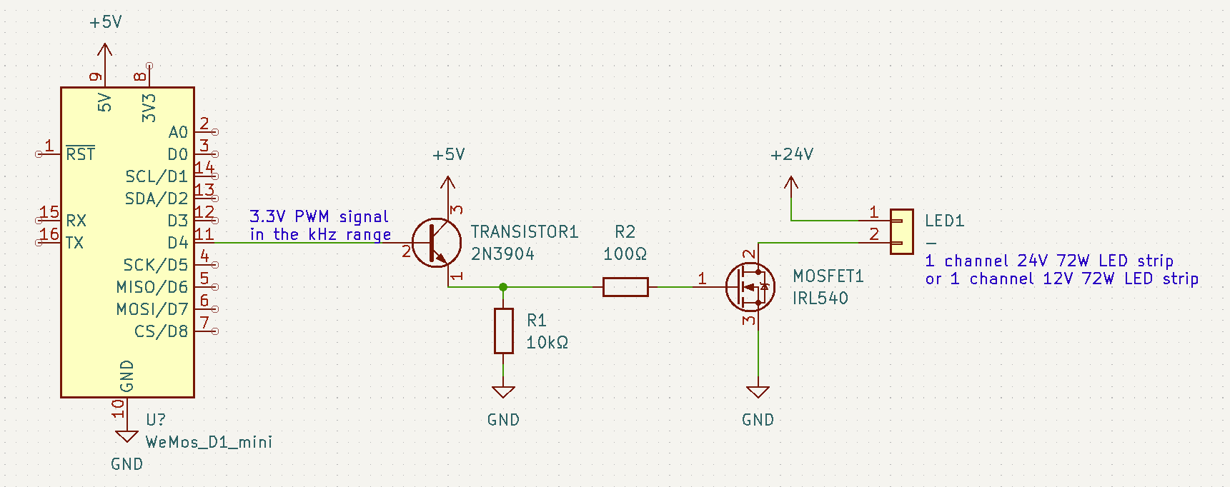
Regarding your proposed circuit, you are operating TRANSISTOR1 as an emitter follower. Its emitter is always 0.7V below the base, so you won't ever have more than 3.3V-0.7V=+2.6V at MOSFET1's gate. That's even worse than just connecting the gate directly to the GPIO pin.
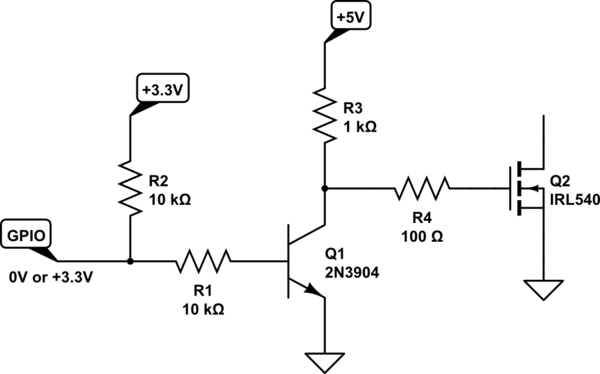
If you want a gate potential of +5V or 0V, then you must configure TRANSISTOR1 as common-emitter, and you must also rename it to Q1, so I don't have to type so much. This kind of thing:

simulate this circuit
This has potential problems:
Q1 is on when Q2 (and the load) is off, so the PWM signal is inverted.
Even with the LEDs off (Q1 is on), there is \$\frac{5V}{R_3}=5mA\$ flowing via Q1.
I don't recommend doing it this way.
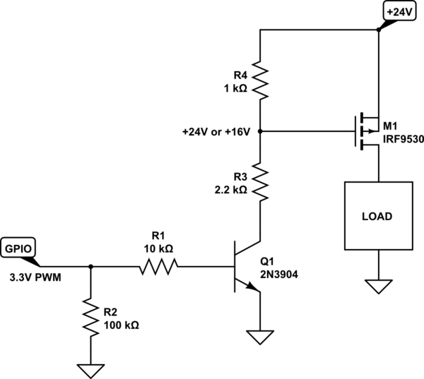
For high side switching, a common-emitter NPN BJT and P-channel MOSFET can be used:

simulate this circuit
This uses R3 and R4 to limit how far gate potential can fall (to about +16V here, for \$V_{GS}\approx 8V\$), ensuring that \$V_{GS(MAX)}\$ is never exceeded. The load is powered when Q1 is on, so there's no signal inversion, and no collector current in Q1 when the load is off. Also, gate charge current is sourced from the +24V supply, offloading the hard work from the MCU to Q1. Since we have a much larger \$V_{GS}\$, MOSFET choice is much less constrained.

