0
\$\begingroup\$

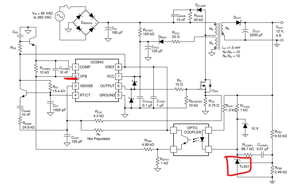
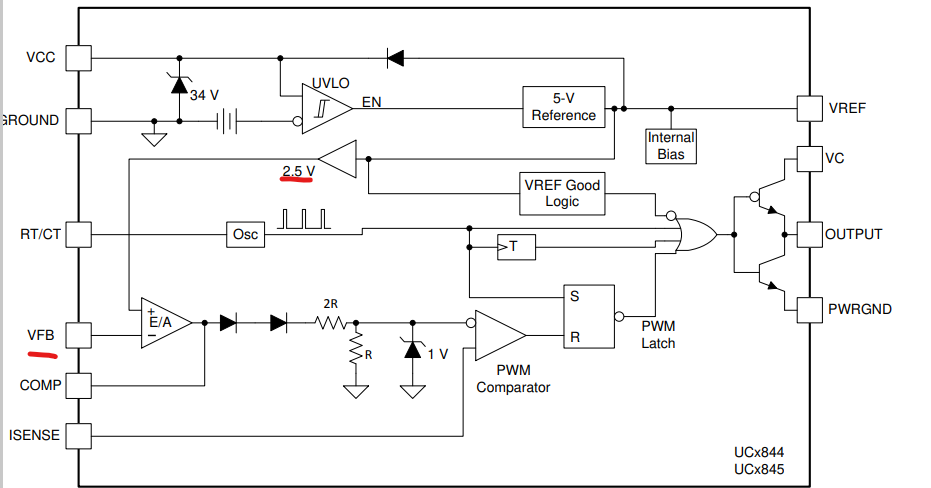
I have a slight confusion regarding the UCC3895, which is a four-channel wave generator. Earlier I had worked on the UC3842 and therefore to see better results I wanted to take a look at the UCC3895. The UC3842 IC has an internal 2.5 V reference voltage set inside the IC so that if the voltage due to the divider on the TL431 changes, then accordingly due to the closed feedback loop it will adjust that voltage and bring it to 2.5 V in order to eliminate the error from the error amplifier:

enter image description here

enter image description here

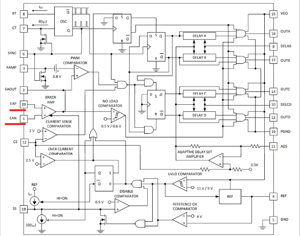
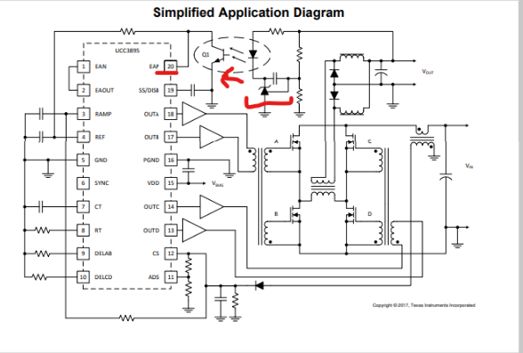
Now moving further towards the UCC3895. In the internal diagram of the UCC3895 I cant find out any internal reference as set here in UC3842 i.e. 2.5 V. There is the same TL431 whose feedback is moving to one end of the error amplifier. How is the IC being able to know its fixed reference? The TL431 just gives the feedback input as done in the UC3842 as well but there was a 2.5 V reference internally and here the reference is missing inside the IC. Previously I asked a similar question but wasn't able to get my confusion clear therefore I wanted to make the question clear.

Kindly help me how the IC is being able to figure out the fixed reference for the IC?

Below are the internal and external complete diagrams:

enter image description here

enter image description here

\$\endgroup\$
2
  • \$\begingroup\$ Hmm, your question is not about the SMPS. But is more about the negative feedback loop. The same principles apply to the linear regulator or even to the amplifier with a negative feedback loop. Did you notice that in UC3842 example circuit the error-amplifier is working as inverting-amplifier? And the optocoupler BJT works as a " emitter follower". Thus, the internal Vref is here "only" to bias the opamp in the linear region. look at this example tinyurl.com/24ut6sqv where bottom BJT act very similar to the TL431. And this is why Vout=(1 + 1k/1k)*2.5V. And this is why Vout = 5V. \$\endgroup\$
    – G36
    Commented Aug 22, 2023 at 17:19
  • \$\begingroup\$ Please cite where your images come from. \$\endgroup\$ Commented Aug 22, 2023 at 20:08

1 Answer 1

1
\$\begingroup\$

First, there is no internal reference in the IC that's being used as part of the control loop.

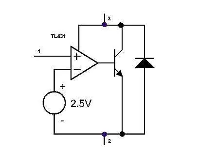
Maybe it will help to look at the equivalent circuit of the TL431 from here. enter image description here

The 2.5 V reference internal to the TL431 acts as the reference for the control loop. The resistor divider from the output of the power supply to pin 1 is compared to the 2.5 V reference. The difference is amplified by the transconductance gain of the TL431. The output current of the TL431 drives the LED of the opto, and the output of the opto is buffered by the internal error amplifier, which in this case is configured as a follower since the error amplifier function (and gain) is provided by the TL431/opto combination.

For non-isolated topologies you could conceivably divide down the IC's internal reference (to meet the common-mode range of the internal error amp) and use the internal error amp to provide loop gain and compensation.

\$\endgroup\$
2
  • \$\begingroup\$ As far as I understood in the UCC3895 we have an external reference of 2.5 due to the TL431 and we are using it in a closed-loop configuration where the error is reduced. But in the case of the UC3842, we have a closed loop TL431 as well as an internal error amplifier. Basically, we can say we have two error amplifiers in that case right? \$\endgroup\$
    – kam1212
    Commented Aug 22, 2023 at 18:49
  • 1
    \$\begingroup\$ Well, yes, in the case of the 3842 the internal amplifier provides additional gain and loop compensation. \$\endgroup\$
    – John D
    Commented Aug 22, 2023 at 19:53

Your Answer

By clicking “Post Your Answer”, you agree to our terms of service and acknowledge you have read our privacy policy.

Not the answer you're looking for? Browse other questions tagged or ask your own question.