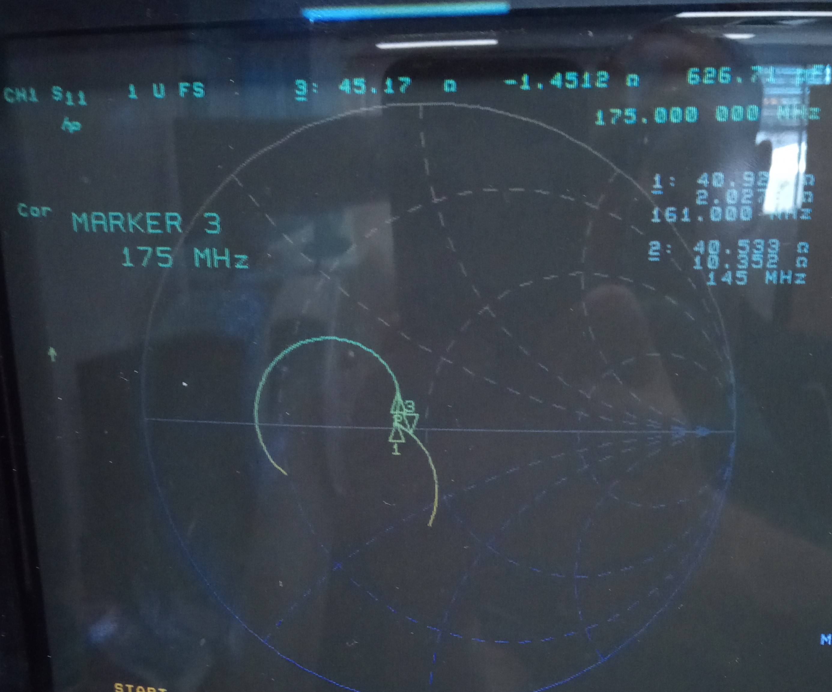
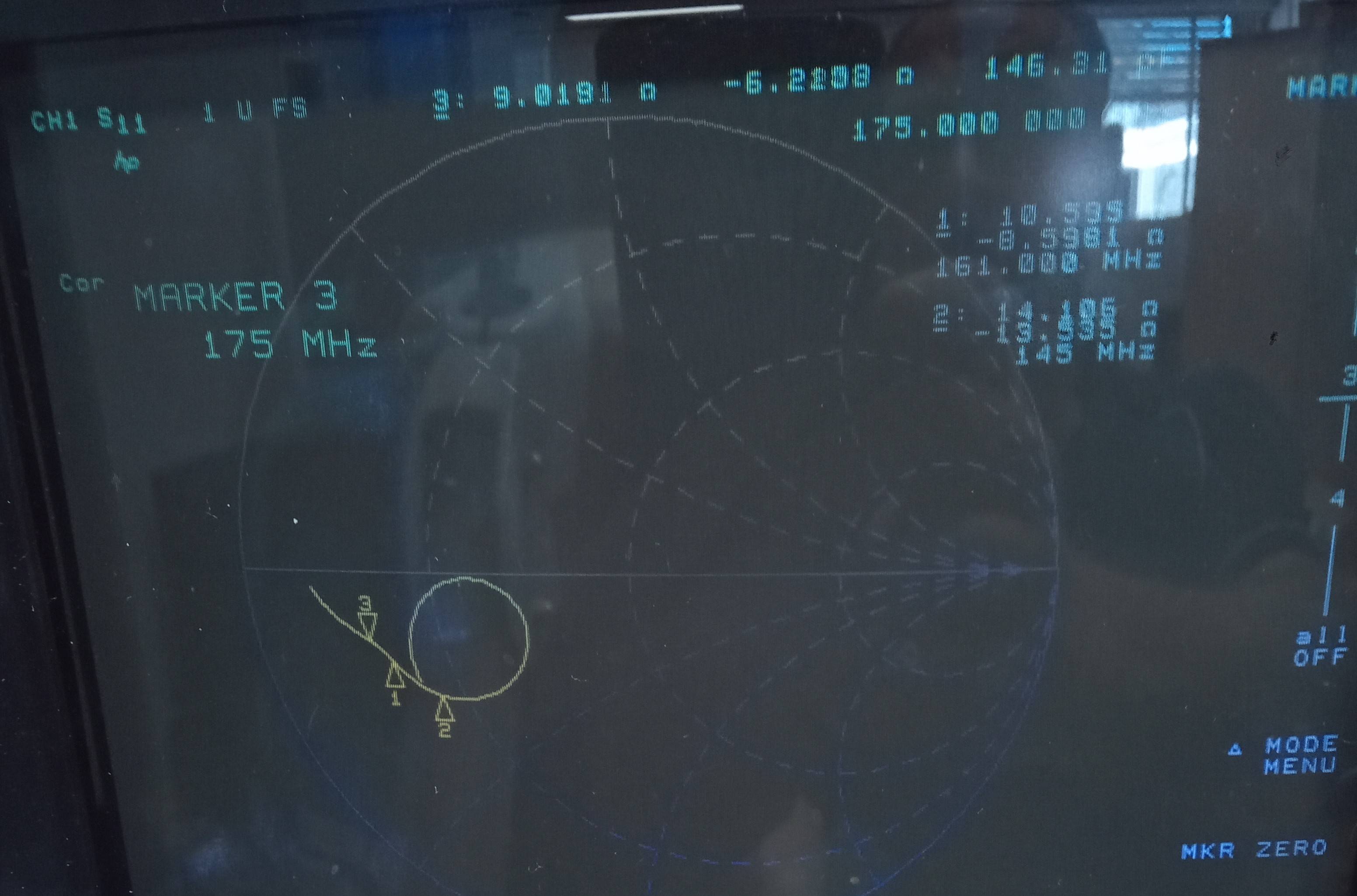
I'm trying to track down a VSWR issue with a RF power amplifier (25 W, 150 MHz). The radio we're using to drive it has a VSWR alarm, which triggers during transmit. Older manufacture runs of the PA don't trigger the VSWR alarm, and I'm not certain that the bill of materials used to build the current manufacture run is correct.
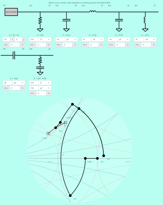
I've entered the power amplifier input circuit to an online Smith chart tool (https://www.will-kelsey.com/smith_chart/) and it shows me the input impedance is nothing like 50 Ω. Given my inexperience with this type of tool, and the experience of the engineer who designed the amplifier, it's more likely an error on my part than on the part of the original designer. I want to confirm that I'm using the tool correctly before I dive in and make wholesale changes.
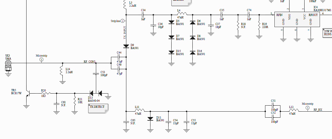
Here is the input circuit. During transmit TR5 switches current through L3-D9-L11-D11, so I've modelled D9 & D11 as shorts. The input impedance to IC4 (RA30H131M1) is 50 Ω according to the datasheet. Receive signal comes through L12 / C51-52.

I modelled the TX detect circuit (D13-TR5) as a 100 pF capacitor in series with 220 Ω to ground, but tried values between 50 Ω and 10 kΩ and didn't see much difference. I left out the 2.2 µH and 1 nF parts as these don't affect the RF performance. This modelled as in an input impedance of 22+16j Ω. I noted that DP5 is close to 50 Ω, If my modelling is correct, then I guess there is a component issue between the input and C34.

So, I have three questions:
- Am I making valid assumptions about the operation of the PIN diodes and large value parts?
- Am I entering the data correctly into the modelling tool (e.g. correct order left-to-right)?
- What is a suitable model for the TX detect Circuit - This has significant effect on the impedance (but I don't think this is the main cause of the mismatch I'm seeing).
As always, Any help is appreciated.


