1
\$\begingroup\$

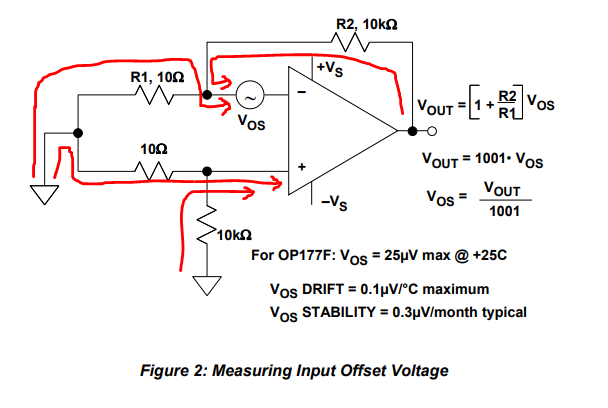
I am reading AD application note MT-037 for input offset voltage measurement procedure.

App note says , measurement will have small error induced due to input bias current .

"For example, 2 nA bias current flowing through the 10 Ω resistor produces a 0.02 µV error referred to the input"

enter image description here

My question is, if the source resistances seen (10||10k) are same for both inverting and non inverting terminal then 2 nA bias currents will generate same common mode voltages (0.02 µV) at inverting and non inverting terminal and eventually get cancelled (CMRR=∞, no mention of CMRR value in app note), then how would they create error in offset measurement?

\$\endgroup\$

1 Answer 1

1
\$\begingroup\$

how would they create error in offset measurement?

We talk about two types of input current usually: -

  • Input bias current (same for both inputs)
  • Input offset current (difference in bias current between the two inputs

So, we can solve the input bias current problem by keeping the resistors associated with each input the same but, we can't solve input offset current problems other than by keeping the net resistance at each input low.

\$\endgroup\$
2
  • \$\begingroup\$ So 2nA is actually 'input offset current' and not 'input bias current' in application note ? it then makes sense as different voltages are generated due to different bias currents values creaing differential mode voltage. \$\endgroup\$
    – Ronnie
    Commented Aug 28, 2023 at 10:19
  • 1
    \$\begingroup\$ I can't help you there because I don't know what you are referring to. I can say that if they say "bias current" then they should mean what I described in my answer but, there's no way I can tell if they made a typo. \$\endgroup\$
    – Andy aka
    Commented Aug 28, 2023 at 10:22

Your Answer

By clicking “Post Your Answer”, you agree to our terms of service and acknowledge you have read our privacy policy.

Not the answer you're looking for? Browse other questions tagged or ask your own question.