To amplify small signals, NPN BJT must be operated such that Vb + VsigLowest must be greater than the voltage drop of Vbe (~0.7V).
How do we center the resulting voltage Vce around 0?
To amplify small signals, NPN BJT must be operated such that Vb + VsigLowest must be greater than the voltage drop of Vbe (~0.7V).
How do we center the resulting voltage Vce around 0?
By "Vce", I assume you actually mean Vc, the collector voltage, and that you want the collector voltage to sit at 0 V when there is no signal, and it goes both positive and negative about this DC operating point.
If all of that is correct, Vc can be centered around 0 V only if the emitter is operating at voltages below GND. IOW, the circuit must have both positive and negative power supply voltages.
There are many common emitter amplifier calculators on the innergoogle, and probably on this site somewhere.
This question about the output part of the simple AC transistor amplifier stage (the coupling capacitor C2) was a welcome addition to me after my yesterday's answer to the question about its input part (the coupling capacitor C1). Thus I have the opportunity to continue here the story that began there.
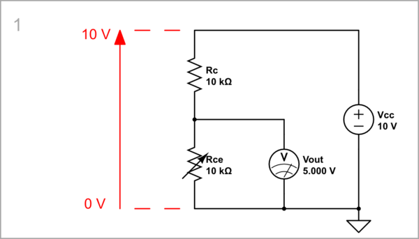
For the purposes of intuitive understanding, we can present the simplest single-supplied common-emitter amplifier by a voltage divider consisting of two elements - the upper "pull-up" collector resistor Rc and the bottom "pull-down" collector-emitter "resistor" Rce.
The voltage divider is supplied only by one positive voltage source Vcc. In this arrangement, when we vary Rce from zero to a very high resistance (100 k in the simulation below), the divider's gain varies from zero to almost 1; accordingly, the output voltage Vout varies from zero to almost 10 V.
simulate this circuit – Schematic created using CircuitLab
We can see this graphically by the help of the CircuitLab DC sweep simulation. Note the curve is non-linear since Rce changes linearly.
As you can see, the output voltage Vout (Vce) is always above ground (positive) since the voltage divider is supplied by a positive power supply.
How do we center the resulting voltage Vce around 0?
To do this (to go below the zero voltage level), it is obviously necessary to include another but negative voltage source. One way is to connect it with its negative terminal to the emitter. In the equivalent circuit, this means to supply the voltage divider with two voltage sources in series (the so-called "split supply"). Now the output voltage can wiggle around ground as OP wants.
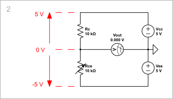
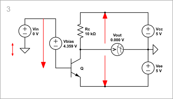
In this arrangement, when we vary Rce from zero to 100 k, the output voltage varies from -5 V to 5 V.
BJT has the problem that both the collector-emitter junction and the base-emitter junction are connected at one common point - the emitter. This requires, because we have "pulled down" the emitter (with -5 V in the schematic below), to "pull down" the base of the transistor by the approximately same amount (of -4.359 V) to bias the input voltage in the negative direction. As a result, the base-emitter voltage is 0.641 V, and the collector voltage is zero.
However, there is another way which is a historical first - instead of "moving down" the emitter, to "move down" (even below ground) the positive collector voltage variations. For this purpose, let's connect a "shifting" voltage source Vc2 in series to the output so that its voltage is subtracted from Vout.
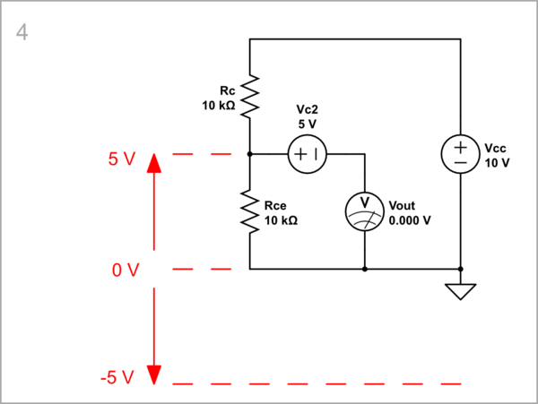
In this arrangement, when Rce varies from zero to 100 k, the positive collector voltage VRce varies from zero to 10 V, and the output voltage across the load (voltmeter Vout) varies from -5 V to 5 V.
Having clarified the concept of "voltage shifting source", let's apply it to build the AC transistor stage from scratch.
The problem of the humble transistor stage is that the input voltage wiggles around (below and above) ground but the transistor wants it to wiggle around 0.65 V.
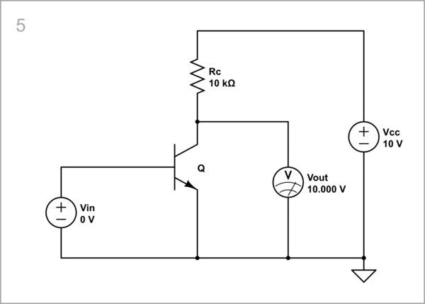
So, if we apply the input voltage directly to the base, the stage will only amplify when the input voltage approaches this threshold.
That's why we "lift" the input voltage by connecting in series a "floating" constant voltage source with Vc1 = 641.5 mV. We can find this value experimentally by opening the Vc1 parameters window and adjusting the voltage so that the output voltage is half of the supply voltage...
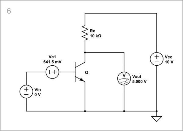
... to vary symmetrically in both directions when the input voltage will be applied later.
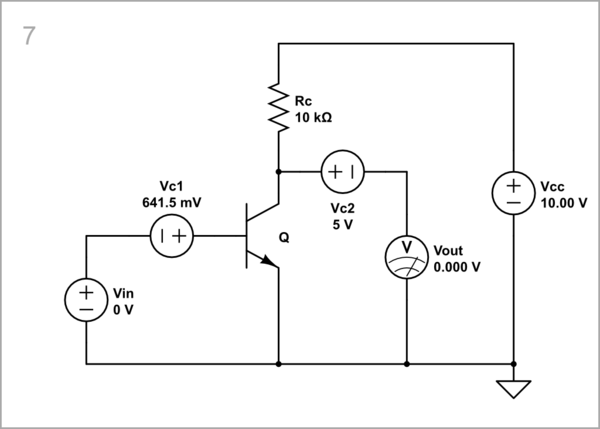
Using the same technique, we "move" the output (collector) voltage by 5 V down by connecting in series another "floating" constant voltage source with Vc2 = 5 V. Let's consider the circuit operation.
Zero input voltage (Vin = 0 V): Basically, the input voltage of the transistor is a sum of two voltages - Vin + Vc1. In this case, since Vin = 0, only Vc1 is applied, and Vce = 5 V (the so-called "quiscient voltage"). The latter is "pulled down" by 5 V; as a result, Vout = 0 V
Positive input voltage (Vin = 5 mV): The transistor lowers its collector-emitter "resistance" so Vce decreases (voltage-divider rule). This change is transferred (reduced by Vc2 = 5 V) to the voltmeter Vout (the load) and it shows a negative voltage (about -1 V here).
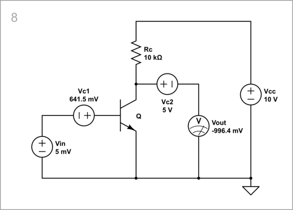
Negative input voltage (Vin = -5 mV): Now the transistor increases its collector-emitter "resistance" so Vce also increases (voltage-divider rule again). This change is transferred (reduced by Vc2 = 5 V) to the voltmeter Vout (the load) and it shows a positive voltage (close to 1 V). The small difference with the previous value can be explained by the transistor nonlinearity.

"Shifting" batteries did a good job of illustrating the idea, but in real circuits they are awkward. For this reason, they were long ago replaced by capacitors that must somehow be loaded.
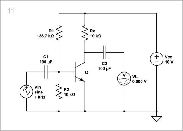
The simplest way to do this in the input circuit is with a resistor Rb connected to Vcc. The C1 charging current passes through the input source, so the latter must be "galvanic". Similarly, the C2 charging current passes through the load that must be "galvanic". An"ideal" voltmeter is not suitable here; so if you open the VL parameters window, you will see that I have reduced its resistance to 10 kΩ.
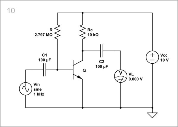
The base resistor Rb has too high resustance so the transistor is sensitive to the harmful effects of temperature, leakages, etc. So, let's replace it with a low-resistance voltage divider R1-R2.
