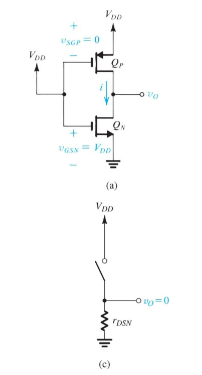
For the output pulled high, my professor's slides give this diagram:

and the equation
$$ r_{DSN} = \frac{1}{k_n'\left( \frac{W}{L} \right )_n \left(V_{DD} - V_{tn}\right)} $$
and for the output pulled low, there's a similar diagram, except that the gates are connected to ground instead of \$V_{DD}\$ and the resistance equation is the same except that the \$n\$'s are replaced with \$p\$'s.
This seems backwards to me though. If I understand correctly, the PMOS is the pull-up network and the NMOS the pull-down. So I would've thought that, when the output is high (i.e. pulled-up), the resistance is determined by the PMOS and vice versa. Why is it actually the opposite?
