1
\$\begingroup\$

I am designing a circuit where I need to do some high side switching to turn on/off the power to a circuit (part of some protection circuitry). This switching is actually very slow and only occurs when a fault is detected such as a short circuit condition.

I could use a P-channel MOSFET and make my life easier, but I don't have any of those in my parts cabinet so I'm stuck using an N-channel MOSFET for high side switching. Obviously I don't want to turn the N-channel MOSFET into a voltage follower so I need to drive that MOSFET with a voltage that is higher than the positive rail.

I looked at a few circuits that could accomplish this task (I was looking into charge pumps to avoid inductors) and came across charge pumps and bootstrapping circuits. I thought both were the same but apparently they are not. Can someone explain the difference between a bootstrap and charge pump circuits? Aren't they the same thing?

enter image description here

\$\endgroup\$
4
  • 2
    \$\begingroup\$ Just a comment, there is also possible to use small isolated converter or power supply to drive the gate. The control signal is transferred via optocoupler. \$\endgroup\$ Commented Sep 14, 2023 at 5:49
  • \$\begingroup\$ I thought about that option as well, but I don't have the components on hand and I only need to turn on/off one mosfets. If i had a circuit with multiple switches then it would definitely be worthwhile to look into that. Also, I'd like to avoid inductors (and transformers), I don't have the materials to build them at the moment. \$\endgroup\$ Commented Sep 14, 2023 at 5:56
  • 1
    \$\begingroup\$ The opto itself can do drive, without a DC-DC at all; if you're just looking for an offhand solution, one could be constructed with a stack of photodiode or phototransistor (base-pin-available type e.g. 4N25) optos... but probably the charge pump is better, yeah. \$\endgroup\$ Commented Sep 14, 2023 at 6:30
  • \$\begingroup\$ What’s your max switch speed? \$\endgroup\$
    – winny
    Commented Sep 14, 2023 at 7:14

3 Answers 3

2
\$\begingroup\$

In common terms (and, I don't know that there's a more complete / strict / technical definition; it doesn't seem it would matter that much, anyway):

A charge pump is an AC-DC or DC-DC conversion unit, distinguished by the use of capacitors and switches to step voltage up or down, typically by small integer ratios. Current handling is generally small, or efficiency poor, due to the capacitor reactance effectively adding with switch and other resistances to constitute voltage drop through the device.

A bootstrap circuit is anything where the traditional phrase "to pull one's self up by your bootstraps", i.e., where some element of the circuit (say, an amplifier) is made to reference its output, thus driving its input, or supply, or other elements, in the same direction; at least momentarily, as long as the bootstrapping element retains its state between cycles.

Clearly, one cannot pull up on their bootstraps forever (or, well, at all, as is the point of the original phrase), so implicit in this application is a time constant, such as how much time the element takes to discharge into the connected circuit.

Typically a capacitor is used to bootstrap a voltage; I suppose an inductor could be used to bootstrap a current just as well, but that's a far less common application.

Since time is of the essence, bootstrapping is typical where cycling, or a return to quiescent conditions, happens regularly. Examples are half-bridge switching circuits (where the low side is always switching alternately with the high side), and amplifiers for various purposes (some early transistorized audio amplifiers saved on then-expensive transistors by replacing a constant-current source with a pull-up resistor, bootstrapped to the output with a relatively large-value capacitor called the "Q capacitor", I suppose because it improved the "quality" of the circuit?).


These are separate applications / perspectives, but there is some overlap. Particularly in the switching circuit (half-bridge inverter), they overlap: the bootstrap is, in a sense, "pumping" charge from the low side to the high side. The difference is, unlike a DC-DC charge pump as such, there is no output rail; the purpose is not to obtain a "VCC + 12V" rail, but to have 12V locally available for the high side regardless of its common-mode (i.e. the MOSFET source) voltage.

So we might not call a bootstrap gate drive circuit a "charge pump" as such.

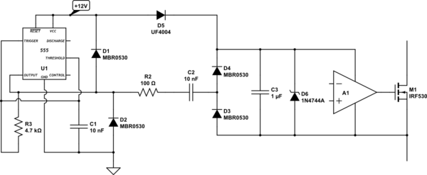
But we can intentionally "pump" charge to the high side, in the event that switching isn't occurring regularly. In this case, we have an AC source located near ground (or, really, anywhere), then connect a series capacitor from the source to the high-side supply. The capacitor gets rectified by clamp diodes, making a "half-wave voltage doubler" circuit (which in this case isn't really "doubling" at all, it's merely copying the peak-to-peak voltage from the low side -- which is to say, merely its supply voltage, no more), and this maintains the high-side drive circuitry in the absence of switching, or an active low-side switch.
schematic

simulate this circuit – Schematic created using CircuitLab

A complete system might look like this. Assuming the MOS source pin voltage is clamped to near GND (i.e. by a low-side MOSFET's body diode, or a flyback clamp diode). Note that, C2 pumps regardless of who (which side) is doing the pumping. As M1 switches on and off, it can deliver many times more charge than the 555 itself does. This would overcharge the bootstrap rail, thus a zener/TVS shall be used to limit voltage to a safe operating level for the MOSFET driver.

The dV/dt (rate of voltage change) can likewise be very high -- suppose the output switches in some 10s of ns, what happens then?! This would draw huge peak currents through C2, hence a series resistor has been added to limit that current, and clamp diodes to protect the 555.

In the event the output is switching regularly, D5 also supplies bootstrap power the normal way. Which itself may want a modest series resistor, to limit startup current, to deal with undershoot/ringing, etc.

Due to the current passing through C2, this strategy is only effective up to modest ratios of supply voltages, that is between gate supply (12V here) and the switching voltage. I've done up to 100V (at 140 kHz) this way before, which was fine, but the design parameters don't look appealing much above there, and I think I would recommend a DC-DC converter for more.

If you can guarantee a slower switching (edge) rate, the voltage ratio can be higher before running into wasted power / component ratings concerns. A slow DC on/off switch, commutating in some 10 µs or so, might be good to a couple hundred volts.

Higher voltages also incur concerns about peak voltages over stray inductances; even at slow rates of change. (And particularly at high currents; consider 100A, or 1000A, commutating in 10µs!). In these cases, total DC isolation may be desirable.

\$\endgroup\$
6
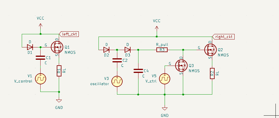
  • \$\begingroup\$ I added a circuit to my original question. Would it be fair to say then that the bootstrap circuit is on the left and charge pump circuit on the right? V_cntrl is the control voltage to turn the mosfet on/off and the oscillator source is supposed to represent the oscillator. \$\endgroup\$ Commented Sep 14, 2023 at 11:09
  • \$\begingroup\$ Left (with minor but necessary additions) is yet a third thing, called a DC restore circuit. Note that the right circuit also needs modifications if VCC > Vgs(max). \$\endgroup\$ Commented Sep 14, 2023 at 13:34
  • \$\begingroup\$ Properly designed charge pumps can be very efficient. They are often a good choice when the equivalent load resistance is high, >1 kΩ. \$\endgroup\$
    – John Doty
    Commented Sep 14, 2023 at 15:31
  • \$\begingroup\$ Hi @Tim Williams, by DC restore circuit, you mean the same thing as a clamper, right? \$\endgroup\$ Commented Sep 14, 2023 at 22:06
  • \$\begingroup\$ @SamuelSnerden Not quite. For an AC input, the peak-to-peak voltage is not clamped. The DC offset is adjusted (restored, you might say) so that it's (mostly) unipolar. \$\endgroup\$ Commented Sep 14, 2023 at 22:36
1
\$\begingroup\$

A Charge Pump is compariable to a DC/DC converter, in that it continuously (with some fixed or variable frqeuency) charges up a cap, switches the voltage at the negativ terminal to the input voltage as well and by that "pumps" the positive terminal to double the input voltage. This high voltage can than be discharged via a diode into an output capacitor.
Advantage: You can draw a continuous output current (as long as the current is sufficiently small, obviously).

Bootstrapping is bascially the same principle, but the capacitor is not switched continuously to keep the charge on the output cap, but the negative cap-terminal gets automatically switches, when the driver output is switched. Only the charge that is momentarily on the cap can be used to drive the higher voltage (most often the gate of a high-side FET). This means, that leakage in the gate will discharge that cap, the voltage at the gate is decreasing over time.
Disadvantage: No continuous output current. You can't keep the transistor on as long as you want. Bootstrapping only works, if the FET is switched with sufficiently high frequency, so that the bootstrapping cap can recharge again and again.

\$\endgroup\$
3
  • \$\begingroup\$ I added a circuit to my original question. Would it be fair to say then that the bootstrap circuit is on the left and charge pump circuit on the right? V_cntrl is the control voltage to turn the mosfet on/off and the oscillator source is supposed to represent the oscillator. \$\endgroup\$ Commented Sep 14, 2023 at 10:09
  • \$\begingroup\$ No, not really. The left circuit would always leave Q1 slightly conductive, it can never fully turn off. The negative terminal of C1 should be referenced to the source of the transistor and the positive terminal can only be connected to the gate when you want to switch the fet on. \$\endgroup\$
    – jusaca
    Commented Sep 14, 2023 at 12:22
  • \$\begingroup\$ Ah yes, I see it now. I need to bring down the gate of Q1 to ground like on the right circuit whenever it needs to be turned off otherwise it's just a voltage follower. If I were to make V_control and V_control' (inverted V_control), and adding a second nmos to pull the gate of Q1 down controlled by V_control' (whenever V_control is low, V_Control' is high). I think a simple astable oscillator will provide both Q and Q' for the V_Control and V_Control' of the left circuit. This will fix it or am I missing something else? \$\endgroup\$ Commented Sep 14, 2023 at 22:00
1
\$\begingroup\$

This switching is actually very slow and only occurs when a fault is detected such as a short circuit condition

In that case you cannot use bootstrapping. With bootstrapping, it is the output FETs that charge the bootstrap capacitor. When the output is low the capacitor is charged, and the subsequent rising of the FET's output takes the capacitor's now large potential difference with it, providing the above-positive-rail gate potential for the upper FET.

This can only happen if the FETs are switching frequently enough that the bootstrap capacitor is recharged regularly. It must never be permitted to discharge significantly while the output is high, since that would cause the upper FET's gate potential to fall to a point where the FET is no longer "over-driven". When that happens, the FET becomes a voltage follower, the very problem you are trying to avoid.

For this reason, you can't use bootstrapping in any switching situation that might have 100% duty cycle (output always high), since the capacitor can't ever charge. That sounds very like your own circumstances.

\$\endgroup\$
5
  • \$\begingroup\$ I added a circuit to my original question. Would it be fair to say then that the bootstrap circuit is on the left and charge pump circuit on the right? V_cntrl is the control voltage to turn the mosfet on/off and the oscillator source is supposed to represent the oscillator. \$\endgroup\$ Commented Sep 14, 2023 at 10:10
  • \$\begingroup\$ @SamuelSnerden Yes, bootstrap left. On the right, oscillator V3 keeps recharging C2, energy which is dumped into C4 keeping it well over Vcc. The left bootstrap has no separate oscillator to do that, so recharging of C1 happens only when V_control goes low. \$\endgroup\$ Commented Sep 14, 2023 at 13:25
  • 1
    \$\begingroup\$ Neither is a bootstrap, as the gate drive isn't referenced to source. \$\endgroup\$ Commented Sep 14, 2023 at 17:20
  • \$\begingroup\$ @TimWilliams Ok, so let me try again and see if I get it right: A bootstrap circuit is a circuit which uses a charged capacitor between the input and output to momentarily pull up the voltage at one end (the input) when the output rises. This capacitor will discharge over time going back to 0. If we want to keep this capacitor charged high, we need to pump charges back into the capacitor as it loses charges over time (such as in your circuit). If that is correct, wouldn't the circuit I posted on the left be a bootstrap circuit like Simon Fitch says, but referenced with GND instead of Source? \$\endgroup\$ Commented Sep 14, 2023 at 22:37
  • \$\begingroup\$ Again, neither makes a connection to the source. The left one requires (VCC+Vgs(on)) volts of drive, and the right one simply makes a (VCC + Vgs(on)) supply, instead of a Vgs(on) supply referenced to source; which means R_pull dissipates much more power. \$\endgroup\$ Commented Sep 14, 2023 at 22:49

Your Answer

By clicking “Post Your Answer”, you agree to our terms of service and acknowledge you have read our privacy policy.

Not the answer you're looking for? Browse other questions tagged or ask your own question.