2
\$\begingroup\$

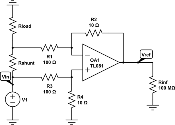
Usually, to measure current in the line the next sch can be used:

schematic

simulate this circuit – Schematic created using CircuitLab

Here Vref is proportional to current through Rshunt as

$$ V_{ref} = I_{shunt} R_{shunt} \frac{R2}{R1} $$

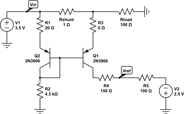
I've seen scheme made on current mirror that has same functionality, but with low latency. But I cannot understand, how does it work:

schematic

simulate this circuit

here $$V_{ref}=I_{R4}\cdot R_4$$ and $$I_{R1} \approx I_{R4}$$

I think that it works as follows: current on both branches is made equal by mirror, while voltage on both is slightly different because of shunt resistance and \$Vref\$ is calculated as voltage divider between \$~Vin\$ and \$V2\$ made by \$R5\$ and \$(R4+R_{Q1})\$ but I don't get how does \$R_{shunt}\$ influence on that value

\$\endgroup\$
1
  • 1
    \$\begingroup\$ This circuit will not going to work as you expected. Take a look here tinyurl.com/yl8vcgu5 \$\endgroup\$
    – G36
    Commented Sep 14, 2023 at 20:09

4 Answers 4

3
\$\begingroup\$

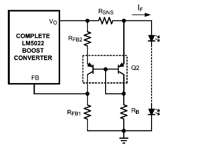
Thanks to G36 for pointing out that the circuit isn't quite correct, the usual approach is shown in this question:

enter image description here

The shunt voltage appears across Rfb2 (KVL around the loop), and neglecting base current Vshunt/Rfb2*Rfb1 appears across Rfb1, which is now a voltage proportional to the shunt current. Q2 serves to bias the primary transistor at an appropriate operating point.

\$\endgroup\$
2
  • 1
    \$\begingroup\$ The circuit as drawn by the OP will not be going to work as desired. Please notice that the larger the load current, the lower the Q1 emitter voltage will be. Thus, the Ic current is smaller and smaller, and the Vout voltage as well. And eventually (for the "high" load currents) the Q1 will be cut off. \$\endgroup\$
    – G36
    Commented Sep 14, 2023 at 19:59
  • \$\begingroup\$ @G36 Thanks, answer updated. \$\endgroup\$
    – John D
    Commented Sep 14, 2023 at 21:02
2
\$\begingroup\$

I'm going to stick with the discrete BJT design you found. It's not bad, despite comments and pointers, otherwise. But it is missing a few details. And I'm going to keep it a single-supply design. No negative rails here.

Before I launch into it, this is actually a complicated product-log problem (as are pretty much all BJT kind of problems, due to the Shockley equation behavior.) So there is a place where I will skate across some details that are kind of important, quantitatively. But I'm doing that because I don't want to dig into the closed mathematical expression, as it involves a function you've probably never heard of (Lambert's W.) So grant me some room there.

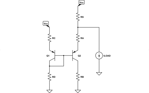
Let's pony up a schematic to talk about:
schematic

simulate this circuit – Schematic created using CircuitLab

Everything happens in an order of magnitude. Good rule of thumb to keep in mind. Either everything happens \$\pm\$ an order of magnitude around a center or else it's just one order.

  • Assume a maximum load current of \$I_{_\text{MAX}}=50\:\text{mA}\$.
  • Assume \$V_{_\text{CC}}=5\:\text{V}\$.

In general, you have to pick a maximum voltage drop for \$R_{_\text{S}}\$ at the worst-case load current. I think a value of \$100\:\text{mV}\$ is usually acceptable. So let's go with that. This means \$R_{_\text{S}}=2\:\Omega\$.

Using the above rule of thumb, we don't want to go less than about \$\frac1{10}\$th of that. So this means that the minimum current through \$R_{_\text{S}}\$ should be about \$5\:\text{mA}\$. That's going to set \$Q_2\$'s quiescent current for us. So when there is no load current at all, that's the emitter/collector current for \$Q_2\$. This means the quiescent (no load) voltage drop across \$R_{_\text{S}}\$ should be \$10\:\text{mV}\$ -- that is consistent with our 'order of magnitude' rule.

We want to trade off voltage across \$R_{_\text{A}}\$ as the voltage drop across \$R_{_\text{S}}\$ changes. So as the drop across \$R_{_\text{S}}\$ goes from \$10\:\text{mV}\$ up to \$100\:\text{mV}\$, the same thing should approximately happen across \$R_{_\text{S}}\$, but in reverse. The problem here is that the BJT (\$Q_2\$) won't cooperate with us. As the current in \$R_{_\text{A}}\$ declines, the \$V_{_\text{BE}}\$ for \$Q_2\$ will adjust itself to oppose that change. There will be about \$60\:\text{mV}\$ change in \$V_{_\text{BE}}\$ for a factor of 10 change in the current (which is what we are targeting due to the rule.) So here is where that Lambert W thing gets in the way. I can just finesse across this and tell you that instead of going from about \$100\:\text{mV}\$ across \$R_{_\text{A}}\$ down to \$10\:\text{mV}\$, it will instead be more like \$100\:\text{mV}\$ across \$R_{_\text{A}}\$ down to \$50\:\text{mV}\$ -- due to the Shockley equation interfering. That's a factor of 5 more than the expected minimum. But this is okay. It just has to be recognized and accepted, is all.

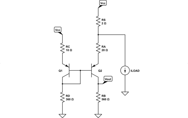
To get a quiescent \$100\:\text{mV}\$ across \$R_{_\text{A}}\$, at \$5\:\text{mA}\$, \$R_{_\text{A}}=20\:\Omega\$. So that's now set in stone, too.

We also now want the sum, \$10\:\text{mV}\$ plus \$100\:\text{mV}\$, across \$R_{_\text{C}}\$. So it is time to consider the left side of the schematic for a moment.

The left side is just two resistors and a diode drop. So very easy to calculate. We should make it semi-stiff, because the base voltage of \$Q_1\$ sets the base voltage for \$Q_2\$. So let's double the quiescent current. (Or more.) Because the sum is \$110\:\text{mV}\$ on the right side, we would like to divide by 11 to keep things easy. So let's set the left side to \$11\:\text{mA}\$. So \$R_{_\text{C}}=\frac{110\:\text{mV}}{11\:\text{mA}}=10\:\Omega\$.

We know that \$R_{_\text{D}}\$ has to pick up the voltage drop, after accounting for the diode-connected \$Q_1\$. At these currents, this is probably close to \$900\:\text{mV}\$ or maybe a little less. But this means that if \$V_{_\text{CC}}=5\:\text{V}\$ then we need to drop another \$4\:\text{V}\$. Roughly speaking, this means \$R_{_\text{D}}=\frac{4\:\text{V}}{11\:\text{mA}}\approx 360\:\Omega\$. So that's set, now, as well.

\$R_{_\text{B}}\$ should be set to handle \$5\:\text{mA}\$ without causing \$Q_2\$ to become saturated. There is already a clue, where \$Q_2\$ resists a bit, that says more than \$1.5\:\text{V}\$ drop has to be handled, so this means \$R_{_\text{B}}\le \frac{3.5\:\text{V}}{5\:\text{mA}}\$. Enough below, to be absolutely sure. So a good value is \$R_{_\text{B}}=560\:\Omega\$.

We now have enough to complete the schematic:
schematic

simulate this circuit

Let's run an LTspice on this:
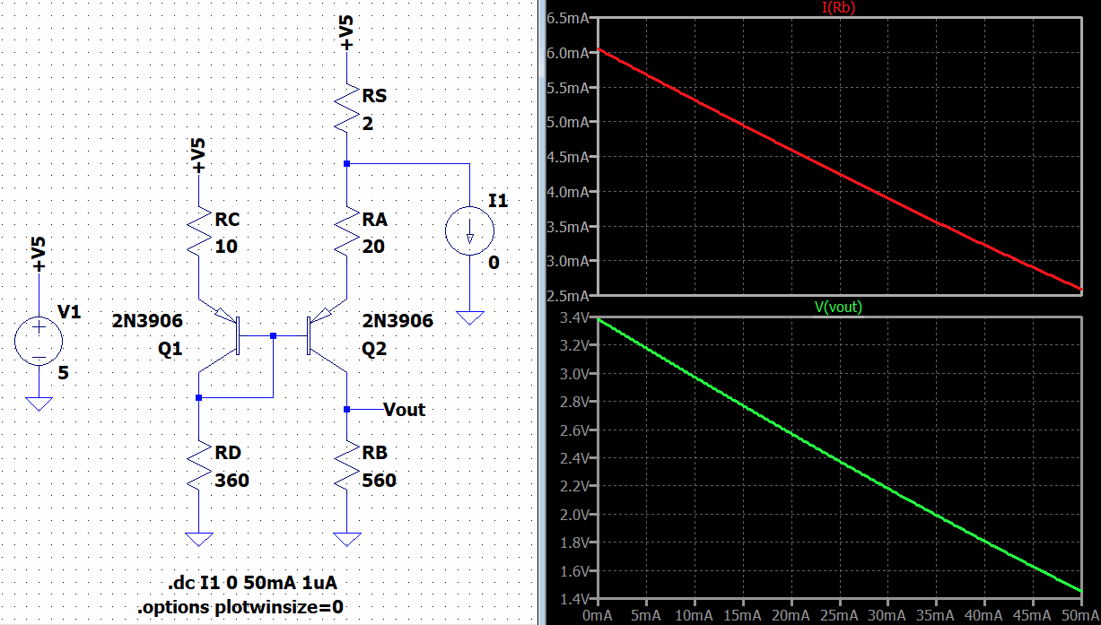
enter image description here

You can easily see that the line is fairly close to linear and that the voltage drops as the load current increases. If this isn't to your satisfaction, you can readily add a current mirror to turn it around and work it, instead, against \$V_{_\text{CC}}\$.

The main point is that the idea can work, after a fashion. And the BJTs stay in their active regions -- no saturated behaviors here.

The key thing to note is that as the voltage drop increases across \$R_{_\text{S}}\$, this drop is partially stolen from the drop across \$R_{_\text{A}}\$ (with the exception to this being that the \$V_{_\text{BE}}\$ across \$Q_2\$ changes with changing emitter/collector current at the rate of about \$60\:\text{mV}\$ per factor of 10 in \$Q_2\$'s current. Since we are pushing towards that much of a change, we can expect a substantial push-back from \$Q_2\$. (This is why we see the minimum current in \$R_{_\text{B}}\$ going to about \$2.5\:\text{mA}\$ rather than the smaller value of \$500\:\mu\text{A}\$ that we would have expected if the Shockley equation didn't get in the way. [There's that factor of 5 I mentioned earlier.] These details can be computed. But the math gets a bit drawn out to get there.)

(Final note: I also didn't account for the base current of \$Q_2\$, which I took to be negligible. One could go further to account for it in the DC biasing. But it's one of those things not worth worrying too much over.)
\$\endgroup\$
2
\$\begingroup\$

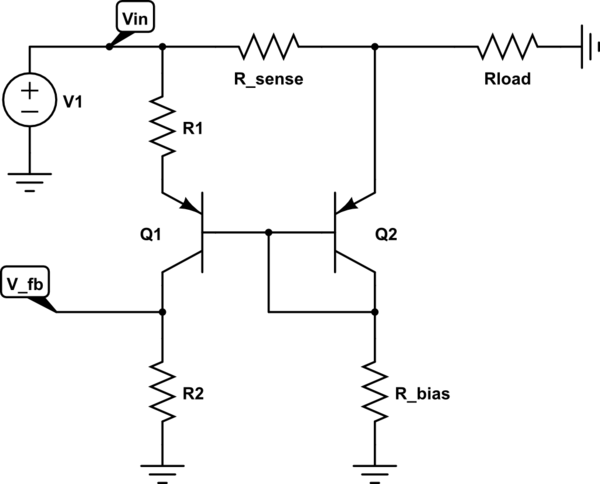
As mentioned elsewhere, there are many ways to approximate a circuit, and each gives some insight into how a circuit works. Here is how I would analyze this circuit to gain insight into its approximate workings.

schematic

simulate this circuit – Schematic created using CircuitLab

I would first note that bases of Q1 and Q2 are tied together. That means the base voltages are the same.

If the transistors are similar, and have similar current, similar temperature, etc, then it is a good approximation that the \$V_{BE}\$'s will be the same.

If the \$V_{BE}\$ of each transistor is the same, then the voltages at the emitters referenced to ground will also be the same.

$$V_{E(Q1)} \approx V_{E(Q2)}$$

From this it follows that the voltage drops across \$R_1\$ and \$R_{sense}\$ must be approximately the same.

$$I_{sense}R_{sense} \approx I_{R1}R1$$

or, rearranged

$$I_{R1} \approx I_{sense}\frac{R_{sense}}{R1}$$

If the base current of Q1 and the feedback current are small in comparison to \$I_{R1}\$

then

$$I_{R1} \approx I_{R2}$$

But

$$V_{fb} = I_{R2}R2$$

So,

$$V_{fb} \approx I_{sense}\frac{R_{sense}}{R1}R2 = \frac{I_{sense}R_{sense}R2}{R1}$$

If we make one more approximation,

$$I_{load} \approx I_{sense}$$

we get an approximate relationship between \$I_{load}\$ and \$V_{fb}\$.

$$V_{fb} \approx \frac{I_{load}R_{sense}R2}{R1}$$

Obviously there have been multiple approximations made, but I think this approach gives rather direct insight into how \$V_{fb}\$ is related to \$I_{load}\$.

\$\endgroup\$
0
\$\begingroup\$

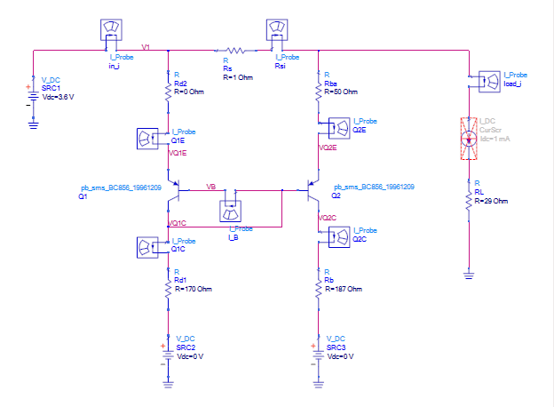
I'd like to thank john-d for the example provided and periblepsis for such a detailed explanation.

Using information from both I've managed to summarize information provided. So... There are two different schemes for my purpose with antogonizing features.

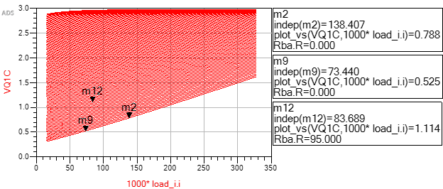
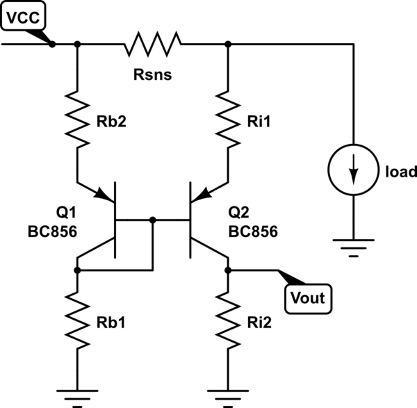
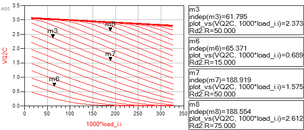
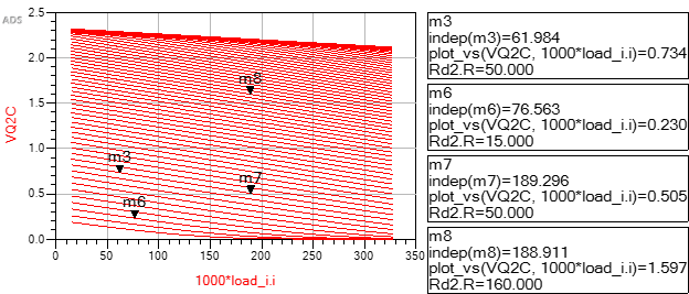
I've made sch in simulator to summarize both and I'd try to explain both:

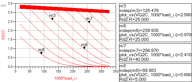
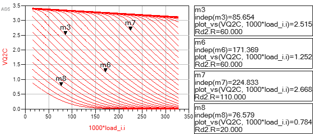
enter image description here

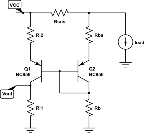
The first one:

schematic

simulate this circuit – Schematic created using CircuitLab

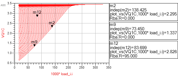
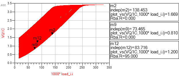
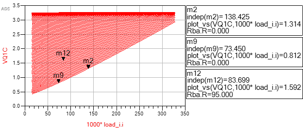
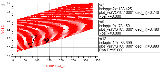
has the next principle: \$R_b\$ has to be chosen to provide the needed bias for Q2 (1mA is enough) while \$R_{SNS}\$, \$R_{FB1}\$ and \$R_{FB2}\$ are used to control the angle of the curve.To calculate needed voltage assume that \$V_{R_{FB2}}\$ = \$V_{R_{SNS}}\$ and you'll get the equation needed to calculate the desired voltage and its behavior when the current changes:

$$ V_{out} \sim I_{load} R_{SNS} \frac{R_{i1}}{R_{i2}} + \alpha R_{ba} $$

where \$\alpha \sim 1/R_b\$

Here are some examples:

  1. \$R_{i1}=1k\$, \$R_{i2} = 50\$,\$R_b=3k\$ enter image description here

  2. \$R_{i1}=1k\$, \$R_{i2} = 50\$,\$R_b=13k\$ enter image description here

  3. \$R_{i1}=1k\$, \$R_{i2} = 100\$,\$R_b=3k\$

enter image description here

  1. \$R_{i1}=1k\$, \$R_{i2} = 200\$,\$R_b=3k\$

enter image description here

  1. \$R_{i1}=1k\$, \$R_{i2} = 200\$,\$R_b=2k\$

enter image description here


I had problems with understanding the second one:

schematic

simulate this circuit

But the idea is close to the same:

  1. set up bias current with \$Rb1\$. I've found, that in this case I need current enough to support right branch but without causing an BJT saturation.
  2. use \$R_{i1}\$ and \$R_{i2}\$ to control incline of V-A curve (and also \$R_{SNS}\$ but nethermind)
  3. use \$R_{b2}\$ to control initial voltage of the \$ V_{out} \$

$$ V_{out} \sim -I_{load} R_{SNS} \frac{R_{i1}}{R_{i2}} + \alpha R_{b2} $$

where \$\alpha \sim 1/R_{b1}\$

Here are examples:

  1. \$R_{i1}=20\$, \$R_{i2}=150\$, \$R_{b1}=300\$

enter image description here

  1. \$R_{i1}=75\$, \$R_{i2}=150\$, \$R_{b1}=300\$

enter image description here

  1. \$R_{i1}=50\$, \$R_{i2}=1k\$, \$R_{b1}=300\$

enter image description here

  1. \$R_{i1}=50\$, \$R_{i2}=1k\$, \$R_{b1}=800\$

enter image description here

\$\endgroup\$

Your Answer

By clicking “Post Your Answer”, you agree to our terms of service and acknowledge you have read our privacy policy.

Not the answer you're looking for? Browse other questions tagged or ask your own question.