1
\$\begingroup\$

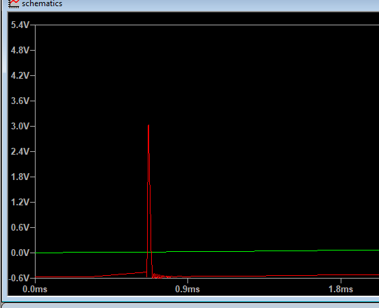
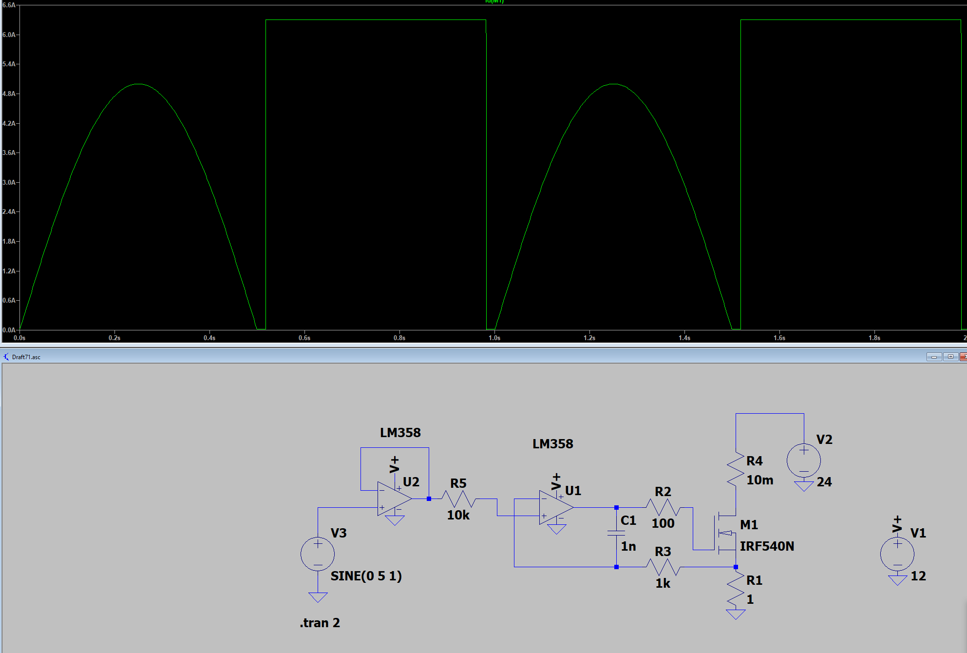
I am working on a DC load circuit and have put together a simple configuration based on templates available online. As you can see in 3rd image attached, I am noticing a small ringing in the load circuit measured at R1 which is a current sense resistor. I am assuming its being generated from the OPAMP not being able to stablise quick enough and so I tried different random solutions like adding 10 pF capacitor between MOSFET base and ground however I am unable to completely get rid of the ringing.

Can anyone suggest a methodological approach to stablise the opamp and remove this ringing?

Thanks,

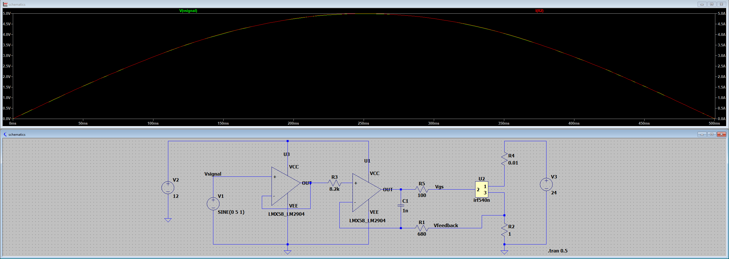
  1. Schematics Schematics

  2. Full output Vsingal vs I(R2)

Full graph

  1. Ringing zoomed Ringing

Edit: Final schematics with added RC filter on 2nd stage opamp to filter out ringing. Adding to original post in case anyone's looking for similar solution:

Final Schematics

\$\endgroup\$
1
  • 1
    \$\begingroup\$ R5 should be much lower ... (100 Ohm or 0 ?). \$\endgroup\$
    – Antonio51
    Commented Sep 17, 2023 at 7:23

2 Answers 2

3
\$\begingroup\$

Here is an additional tweak that will help ensure stability.

enter image description here

The output in my simulation above is more-or-less accurate if V3 is current-limited. In reality U2 will be destroyed if V3 is too low in source impedance.

You should limit the input voltage to U2 to >= 0V. If it goes negative by more than a few hundred mV and the current is limited you'll see the phase reversal in my simulation, and if it's not limited you'll probably damage the chip.

\$\endgroup\$
5
  • \$\begingroup\$ Thanks for your response. It seems the 1nF capacitor and changing R3 to 680 ohms did the trick. I am now getting full current resolution without any ringing. Regarding the V3, I am only using sine wave to test the characterstics of variable DC input. In real world it will be 0 - 5VDC and thus my input reference will never go in negative. \$\endgroup\$
    – Prashant
    Commented Sep 17, 2023 at 13:23
  • \$\begingroup\$ Also, may I ask the theory behind the capacitor and resistors (R2, R3 and C1) and how's it helping eliminate the ringing ? My understanding is that the three elements create a RC filter which elimitated the harmonics (ringing). Is my assumption correct ? \$\endgroup\$
    – Prashant
    Commented Sep 17, 2023 at 13:27
  • 2
    \$\begingroup\$ @Prashant Capacitive loading (such as the gate in the MOSFET with only 1Ω in series effectively) can destabilize most op-amps. The series resistor makes it much worse (the op-amp itself has poorly documented ~100Ω output resistance). By adding significant phase-shift to the feedback you're (at a minimum) decreasing phase margin. The theory behind in-loop compensation such as I used is covered in this AD paper, but note that it's somewhat guesswork since the output resistance is not well known. \$\endgroup\$ Commented Sep 17, 2023 at 14:06
  • \$\begingroup\$ To test this (including in simulation), you should use square waves which are much more likely to excite oscillation or ringing than sine waves. \$\endgroup\$ Commented Sep 17, 2023 at 14:07
  • 2
    \$\begingroup\$ I feel like I'm learning more from just being on this forum then my entire 4 yrs of engineering. Thanks a lot for clear , crisp and real-world explaination for this problem. \$\endgroup\$
    – Prashant
    Commented Sep 17, 2023 at 14:32
3
\$\begingroup\$

Here is what you should have as outputs ... when changing your R5 to 100 Ohm.

enter image description here

Here is the "response" with a square wave at 10 kHz.

enter image description here

\$\endgroup\$
1
  • \$\begingroup\$ Thanks for the suggestion. Replacing R5 to 100 ohms did help a bit. \$\endgroup\$
    – Prashant
    Commented Sep 17, 2023 at 13:24

Your Answer

By clicking “Post Your Answer”, you agree to our terms of service and acknowledge you have read our privacy policy.

Not the answer you're looking for? Browse other questions tagged or ask your own question.