2
\$\begingroup\$

Related to my previous questions, I would like to know what the approach for determining the loop gain and transfer function of the circuit presented below is:

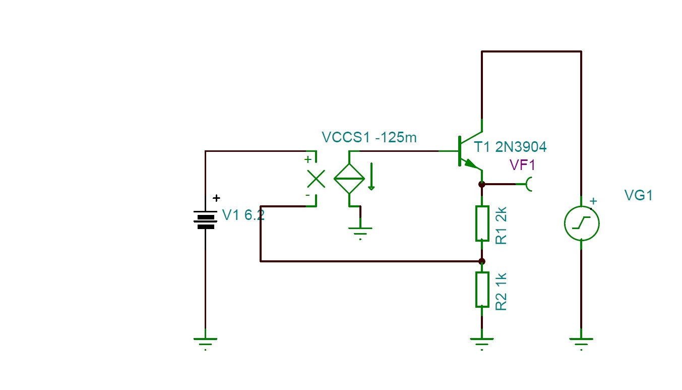
enter image description here

The circuit is highly simplified. The VCCS would in reality be a differential amplifier loaded by a current mirror and would have big input and output impedances. VG1 is meant to represent the unregulated input voltage of the regulator with a DC level and a significant AC ripple. V1 would also be a Zener voltage reference.

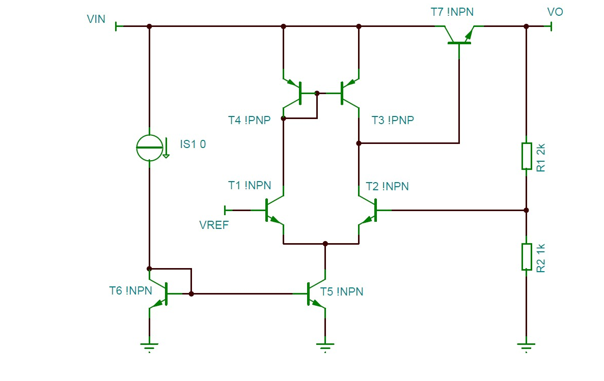
This representation is closer to the reality of the circuit:

enter image description here

For DC conditions I calculated the closed loop gain to be:

$$V_{o}=\frac{g_{m}(\beta + 1)(R_{1}+R_{2})}{1+g_{m}(\beta + 1) R_{2}}\cdot V_{ref}$$

Simplifying for

$$g_{m}(\beta + 1) R_{2}\gg 1$$

gives the usual

$$V_{out}=\left(1+\frac{R_{1}}{R_{2}}\right)\cdot V_{ref}$$

For the low frequency closed loop gain / open loop gain the result is the same. I obtained it by breaking the loop, passivizing all DC sources and replacing the transistor with the small signal equivalent model.

I am almost certain I made some mistakes in my derivations.

What is the correct approach?

\$\endgroup\$
2
  • \$\begingroup\$ Question: Please, give some information about the voltages Vin and Vo (second diagram). \$\endgroup\$
    – LvW
    Commented Nov 2, 2023 at 9:26
  • \$\begingroup\$ Vin is a 20V DC source with a 5Vpp AC ripple. Vo is the regulated output voltage. \$\endgroup\$ Commented Nov 2, 2023 at 10:01

1 Answer 1

1
\$\begingroup\$

Here is my approach for a (rough) loop gain calculation:

  • The loop is opened at the base node of T2

  • The voltage gain at the collector node of T2 is

    G=v_c2/v_b2=-(1/2)gm_2 * r_load * 2=-gm_2 * r_load. (the factor 2 results from the current mirror)

  • The dynamic load resistance is r_load=hie_7(1+gm_7 * R_e) with R_e=R1+(R2||r_in2)

  • Because of the voltage follower (T7) we can set v_c2=v_e7 and the voltage v_f across the feedback resistance r_f=(R2||r_in2) can be found using the voltage division between r_f and R1.

  • Therefore, the loop gain is G_loop=G * [R2||r_in2]/[R1+(R2||r_in2)]

\$\endgroup\$
3
  • \$\begingroup\$ I needed some time to run this in my head. If I understand correctly, you detach the loop at T2 and add a test voltage source at its base: v_b2. What I don't understand is why the loop gain is v_f / v_b2 and not v_out/v_b2. I know you are right, but it still puzzles me. \$\endgroup\$ Commented Nov 3, 2023 at 10:46
  • \$\begingroup\$ I have opened the loop at the base of T2 for applying a test signal. To get the loop gain I must consider the other end of the opening as the loop output - and that is the voltage I have called v_f because this voltage is fed back to the base of T2. \$\endgroup\$
    – LvW
    Commented Nov 3, 2023 at 11:50
  • \$\begingroup\$ I fully understand now. Thank you! \$\endgroup\$ Commented Nov 3, 2023 at 12:52

Your Answer

By clicking “Post Your Answer”, you agree to our terms of service and acknowledge you have read our privacy policy.

Not the answer you're looking for? Browse other questions tagged or ask your own question.