Problem overview
I am designing a multi-board pulser device for ultrasound, and am encountering a conceptual issue when trying to prevent a ground loop in this device. I added a minimal example to show what the problem is. Possible solutions and why they might or might not work are listed at the end of the post.
Detailed Description
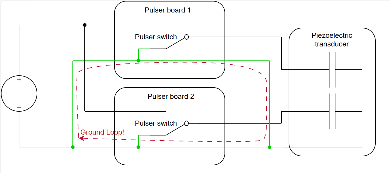
My simplified circuit consists of one power supply providing 50 V to two separate pulser boards. Each pulser board produces a 10 MHz square wave with a peak-to-peak amplitude of 50 V for a few cycles. This square Wave excites the two elements piezoelectric transducer (PZT) that will then emit ultrasound. In addition to the pulser, each board mounts a sensitive ADC that will read the response of the PZT for the reflected ultrasound transmission (this part is not depicted in the image).
Issue description:
as the ground plane of the piezoelectric transducer is shared for the two elements, for this basic circuit layout it is impossible to create a star ground at the power supply. Due to the high current impulses that the system will emit, I fear that this, even with aggressive signal decoupling, will lead to significant noise that would affect the ADC and reduce its precision
Nonviable solutions:
- Mounting everything on a single board: Viable for the toy example but not in real life, as the real system will have a too high number of channels to physically fit them all on one board.
- Providing each board with its own isolated power supply: partially viable, but will increase a lot the complexity of the design. In addition to that, the ADCs on each board have to be supplied from a centralized source as it is not possible to isolate their digital output, so managing the ground plane crossings would be a huge headache
Possible solution (?)
Filtering both the power and ground connection for each pulser with a common mode choke/ ferrite or similar. This would create a high impedance path for the high frequency return current from the PZT, but a low impedance path at DC to supply the pulsers. Possible problems: communication with the pulsers is also fairly high-frequency (100 MHz), so something such as a digital isolator might have to be used.
Question:
What do you think is the best way to solve this problem? Is there some alternative strategy that would work well? If my possible solution could work, what are issues that could arise with it?
EDITS here:
Answer to questions in the comments:
Q: Do time of emission and time of measurement overlap?
A: No, but they are very near to each other. Measurement starts 1 us after the end of emission. The ADC might still be saturated at that point if the noise emission is too high (indeed, in a previous design it is).
Q: I'm really unsure as to what the problem is that your are describing or whether it is something that you think might be a problem.
A: I think it might be a problem. What I am looking for is more experienced engineers than me to give me some pointers about where to look to find a solution, mitigation, or to tell me not to worry too much :). I found it hard to be more succint than this, indeed it seems like I did not include enough information about some crucial part of the problem.
Q: Where is the ADC in your picture?
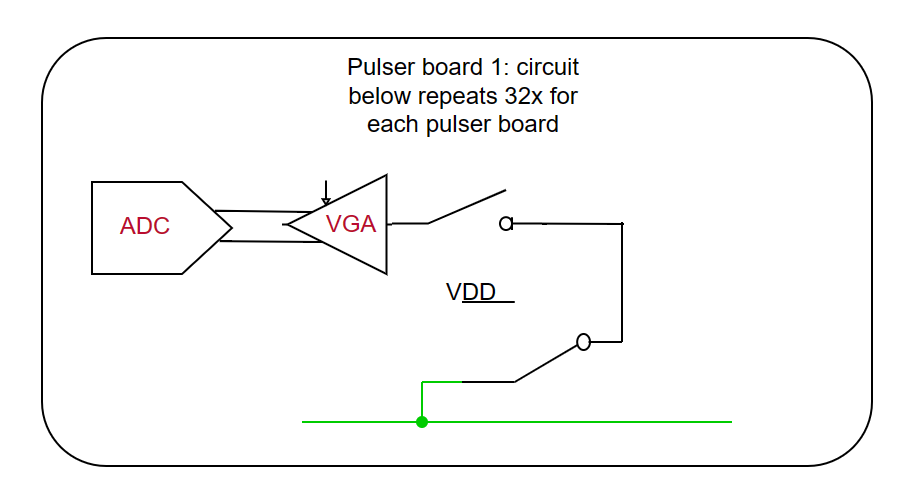
A: the ADC is connected through a switch to the pulser as in this picture:

Q: What do you think is going to cause the ground loop current to flow in your picture?
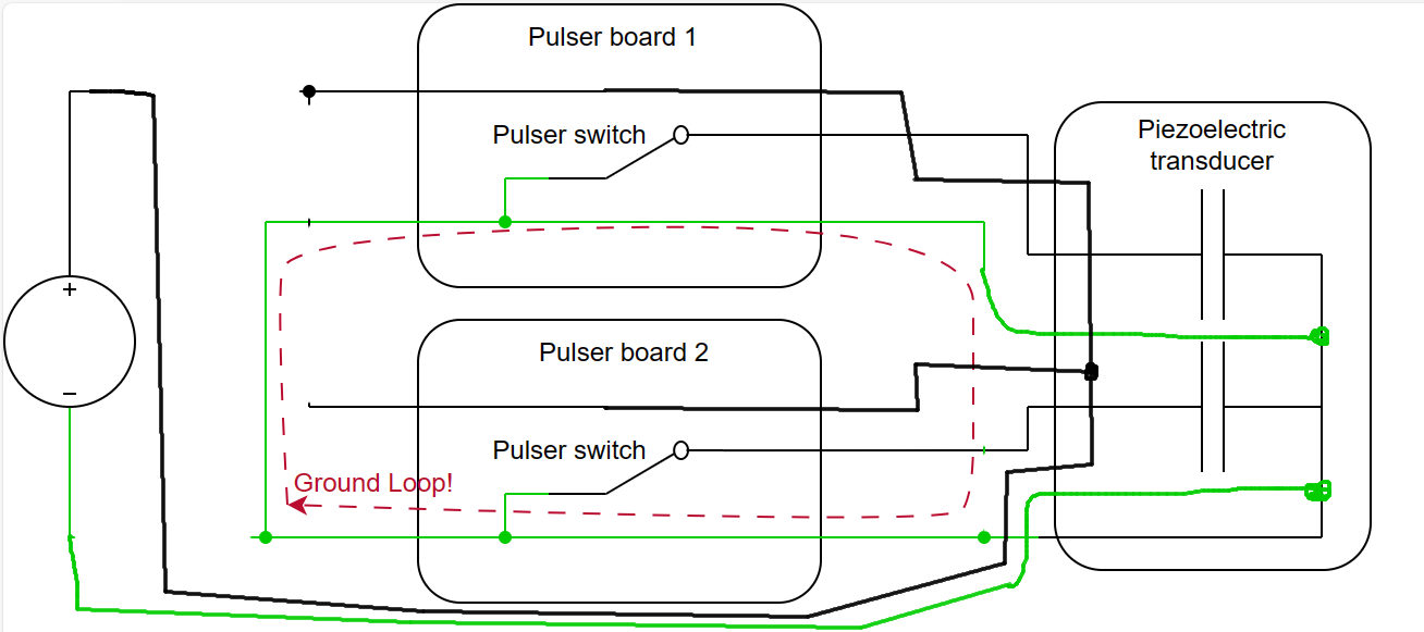
A: all ground connections are going to have a very low impedance both on the transducer and on the power supply connection side. This means that I could design this system in a way that a significant amount of current from the pulse flows back over the backplane connector (left side) rather than from the transducer connector (right side). My boards will also contain digital interfaces for the pulser and ADCs (QSPI, differential @ 100 MHz and JESD204B, differential @ 10 GHz) that will be connected over the backplane connector, and these could be affected from stray currents.
Q: Can you separate the returns for the two transducers? What you described in your answer to the preceding question just means that the current is going to flow along multiple paths; not that you're going to have circulating current.
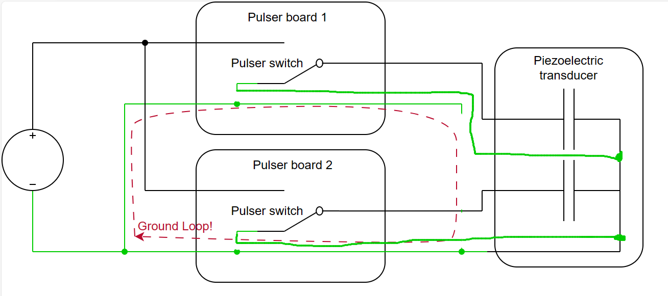
A: Not really, the transducer is built with PZT elements on a single contiguous ground plane. True, there will be no circulating current. I am mostly worried about the EMI emission of the longer return path. A previous test design by another engineer with a similar structure had severe EMI issues, making the design almost unusable. The problem is that the stimulation is quite high-powered (up to 100V and 1 A at 10 MHz per element, times 256 elements) and the ADCs have to detect signals in the order of microvolts and have to be placed rather near to the pulsers on the pulser boards.


