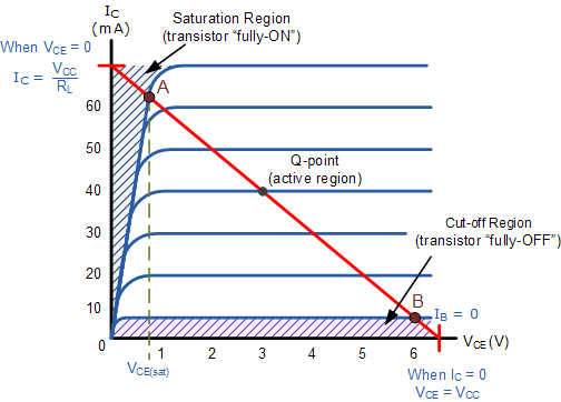
The graph you gave us is quite difficult to interpret in terms of reverse or forward bias states of the junctions, because it doesn't show collector, base and emitter potentials with respect to each other. You have to infer such information. I explain this in detail in another answer here.
To confuse even further, there are subtle hints in the graph you show us that a collector resistor is present in the test setup. Statements like \$I_C=\frac{V_{CC}}{R_L}\$, and \$V_{CE}=V_{CC}\$, in my opinion only serve to confuse. They might be true, but the context is misleading. Again I refer you to my other answer.
It's impossible to show the cut-off region in that graph to a realistic scale. If you look at that red-shaded cut-off region, it seems to indicate that collector current \$I_C\$ will be about 7mA in cut-off.
That's not realistic (except for certain specialised BJTs), because in cut-off, collector current is more likely to be microamps or nanoamps, depending on the model. It's not possible, with a Y-axis scaled in milliamps, to clearly represent such a small area, and so this area is grossly exaggerated in the graph.
In this pedagogical context, I would argue that a collector current of 7mA is very far from cut-off, and the graph is misleading, but I understand why the exaggeration was necessary. In reality, you'll have a hard time finding a bipolar junction transistor whose collector current is millamps, when base current is zero.
So, if that graph isn't very helpful in the context of your question, we require a setup that does a better job, and can provide us with a graph showing clear transitions from one regime to another, while also showing the potentials of base, collector and emitter, to enable us to determine the biasing state of the two junctions:

simulate this circuit – Schematic created using CircuitLab
Take a look at base (blue) and collector (orange) potentials as I sweep V1:

The emitter is obviously held at 0V throughout.
In the region to the right of the right-most green marker, this is saturation. It is marked by the instant that collector potential falls below the base, causing the base-collector junction to become forward biased.
It is still possible for collector potential to continue to fall, approaching the emitter, but in practice it can only fall to within 0.1V or so of the emitter.
Your tutor is therefore correct to suggest that the state of saturation begins when both junctions are forward biased. Collector potential has fallen below the base, causing the B-C junction to be forward biased, even if only slightly, and the B-E junction is also still forward biased.
The state of cut-off is everything to the left of the left-most marker. Its precise position is debatable, since "cut-off" could be defined in different ways. Perhaps it means the state where collector current is insufficient to "operate" the load. Perhaps in some particular application it means the state where collector current is below 1% of saturation current. The definition of cut-off depends entirely on who you ask, and the context of the application.
However, in that graph, cut-off clearly ends somewhere in the region where collector potential begins to fall from its maximum of 3V. This is when collector current begins to rise from near-zero:

To the left, then, collector potential is always greater than the base, so in cut-off we can state correctly that the base-collector junction is reverse biased. However, the bias state of the base-emitter junction isn't so clearly defined. That can be reverse biased, or even slightly forward biased, without causing significant collector current. Cut-off ends when the base-emitter junction begins to conduct significant base current, which varies, but in general occurs somewhere near \$V_{BE} = 0.6V\$.
I think it's more accurate to say that both junctions reverse biased will create a cut-off state, but the B-E junction can even be slightly forward biased without leaving the cut-off state.


