Transistor biasing techniques
From the side of the base (by voltage)
It is widely used in single-ended AC amplifiers. In this configuration, a biasing voltage divider with a relatively high output resistance is connected to the transistor base. The AC input signal is applied through a coupling capacitor to the base so it is added to the bias voltage.
Actually, two voltage sources - DC biasing and AC input, are connected in parallel. The former is imperfect (with some internal resistance), the latter is perfect (with very low impedance) so its voltage dominates.
A problem of this biasing technique is that the voltage divider shunts the input of the CE transistor amplifier. Another, even more fundamental problem is that a DC voltage source (not containing an internal capacitor) cannot be connected directly to the amplifier input because it will suppress the divider bias voltage and impose its voltage. Therefore, it is desirable to bias the transistor from the side of the emitter.
From the side of the emitter (by current)
But we cannot bias the transistor from the emitter side with a voltage because in some cases the emitter voltage must vary; so in these cases we would have to bias it through current. But in a single-ended stage this is not possible because the emitter voltage will not be fixed but will follow the base voltage, and the collector current will not change.
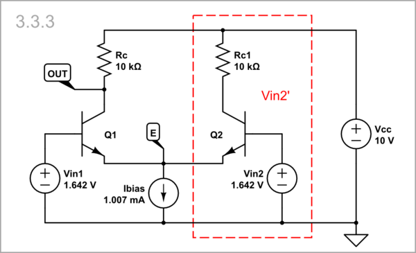
For this purpose, the differential stage was invented where a second transistor (emitter follower) is connected "in parallel" to the first (i.e. their emitters are joined). In this configuration, a current source and two “voltage sources" are connected in parallel, and act as follows:
Common mode: When the two input voltages simultaneously vary in the same direction, the emitter voltage follows them but the current source passes a constant bias current through the emitters. The collector currents and the collector output voltage do not change.
Note that the current source cannot directly draw bias current from the emitters; it only "indicates" that it wants to do so by starting to "pull down" the emitter. The transistor "senses" the voltage drop, and according to the negative feedback mechanism, begins to "pull up" the emitter to restore the voltage. However, this requires a corresponding base current, the path of which must be closed through something - the input voltage source which must be able to pass DC.
Differential mode: When the two input voltages simultaneously vary but in opposite directions, the emitter voltage stays constant (virtual ground). The collector currents and the collector output voltage vigorously change.
CircuitLab experiments
Let’s now explore these biasing techniques by the help of CircuitLab.
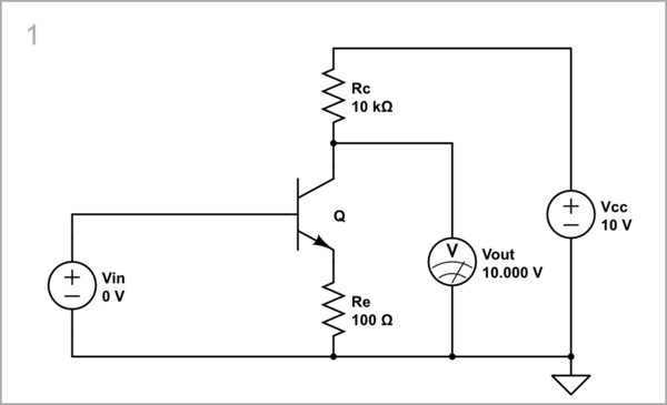
No biasing
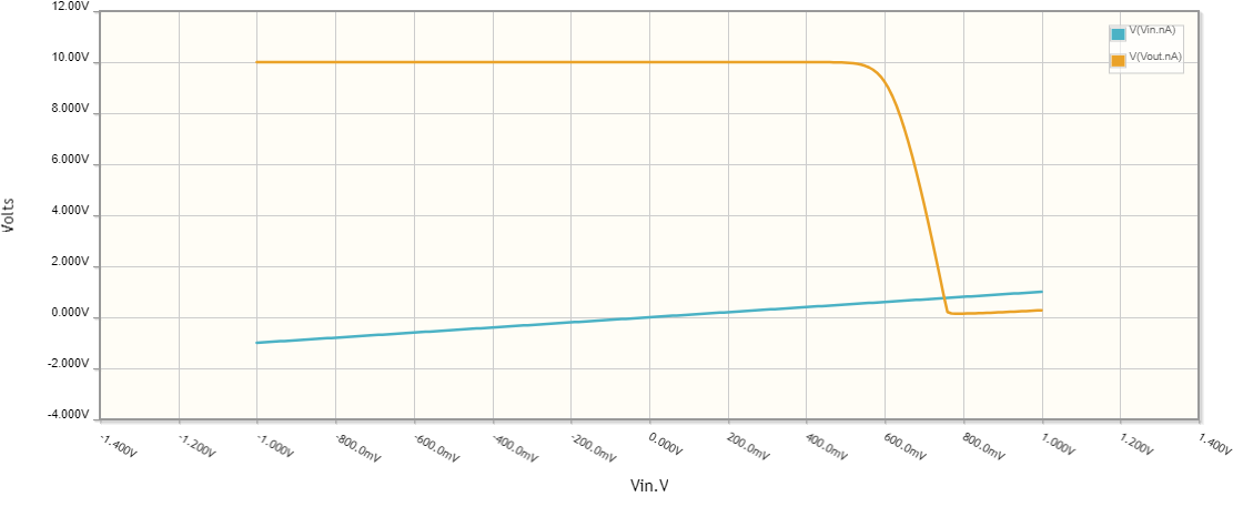
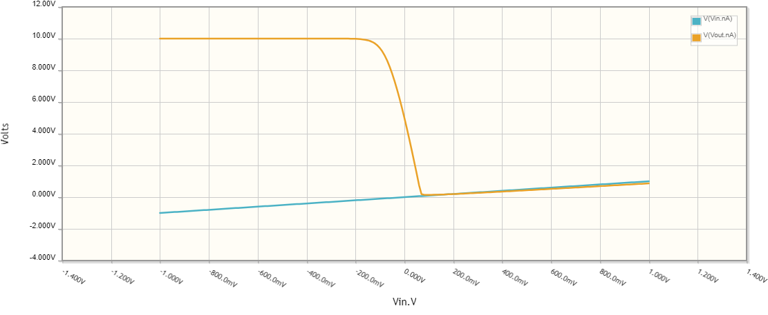
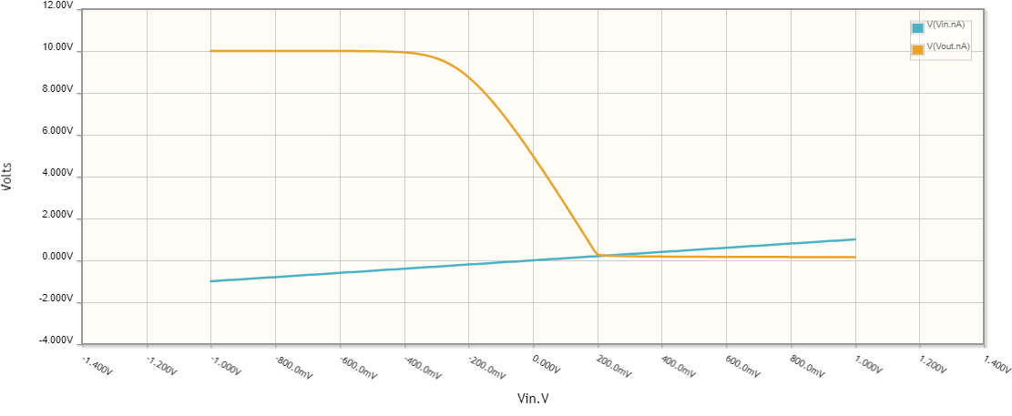
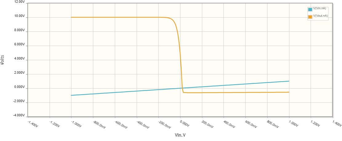
The problem with the transistor is that it operates in a very small input voltage range (about 200 mV). We can explore it by "sweeping" Vin (run the CircuitLab DC Sweep Simulation).

simulate this circuit – Schematic created using CircuitLab
So, when the input voltage changes from -1 V to 1 V, the transistor properly works (amplifies) only in the region from 600 mV to 800 mV.

Therefore, we need to "lift" the input signal applied to the base-emitter junction and limit its variations within 200 mV. We can do it in two ways - by adding the bias voltage to the base or by subtracting it from the emitter.
Biasing from the base side
In series: The obvious way to sum the voltages of the two sources is to connect them in series. We can connect them in two ways, but always one of the two sources is "floating", which creates inconvenience.
Grounded bias source, floating input source: It can be used with floating voltage sources such as microphones, sensors, etc.

simulate this circuit
Grounded input source, floating bias source: This configuration is used in AC amplifiers where the coupling capacitors act as floating Vbias sources.

simulate this circuit
As you can see, the amplifier transfer curve is symmetrically located with respect to the zero voltage point.

In parallel: Let's try this option as well, even though it seems impossible.
Conceptual circuit: The simulator does not allow "ideal" voltage sources to be connected in parallel; so let's set some very small resistance (1 Ω) to one of the two sources (Vbias).

simulate this circuit
As you can see, Vin dominates over Vbias, and actually there is no biasing.

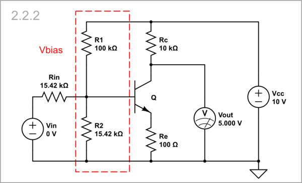
Voltage divider: So Vin should be connected through another resistor Rin to the base. Vbias can be implemented by an R1-R2 voltage divider. Thus the three resistors form a resistor summer with weighted inputs that sums Vin and Vbias.

simulate this circuit
The disadvantage of this resistor coupling is that the input voltage is attenuated, and the gain is decreased (the transfer curve is steeper).

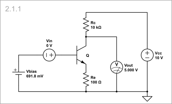
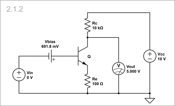
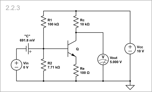
Coupling capacitor: There is no such a problem if Vin is connected through a charged capacitor. For convenience, we can simulate it in a DC manner by a "rechargeable battery" without worrying about time and frequency). Note that actually the coupling capacitor is connected in series to Vin like in the Schematic 2.1.2 above.

simulate this circuit
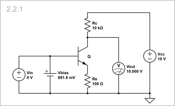
The transfer curve is the same as in the Schematic 2.1.1.

Biasing from the emitter side
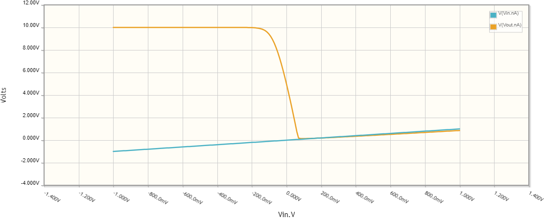
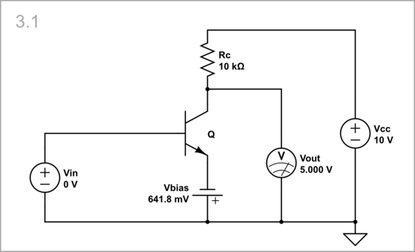
By voltage: We can place Vin and Vbias on either side of the base-emitter junction; so they are effectively connected in series as in the Schematic 2.1.2 above. An advantage of this connection is that both voltage sources are grounded.

simulate this circuit
Note that the gain has increased because there is no negative feedback (resistor) in the emitter.

So the emitter will be at permanently fixed voltage Vbias which is not always desired. For example, in a differential amplifier, we want in some cases (single-ended and differential mode) the emitter to be "fixed" and in others (common mode) to be "moving".
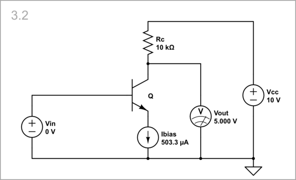
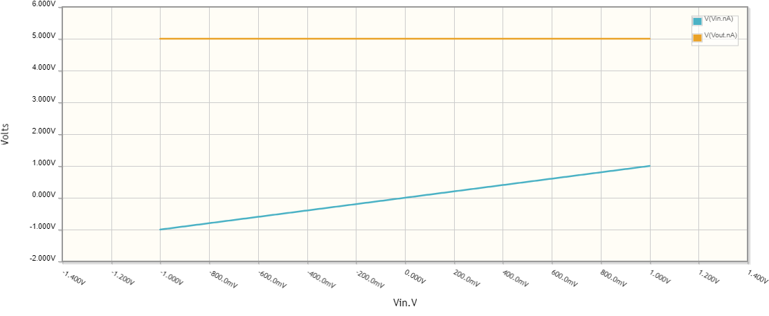
By current: Then let's try to bias the transistor by injecting a bias current into the emitter. Thus the emitter will be "movable" (Vin can easily change its voltage).

simulate this circuit
The emitter voltage changes, but the emitter current and, accordingly, the collector current and the voltage drop across Rc does not change... so there is no gain.

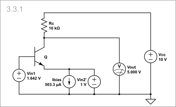
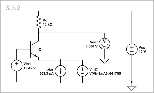
Through one or the other: But how to do so to switch the mode? And here comes the ingenious "long-tailed pair" idea - to connect another voltage source Vin2' in parallel to the other voltage source Vin1 and the current source Ibias.
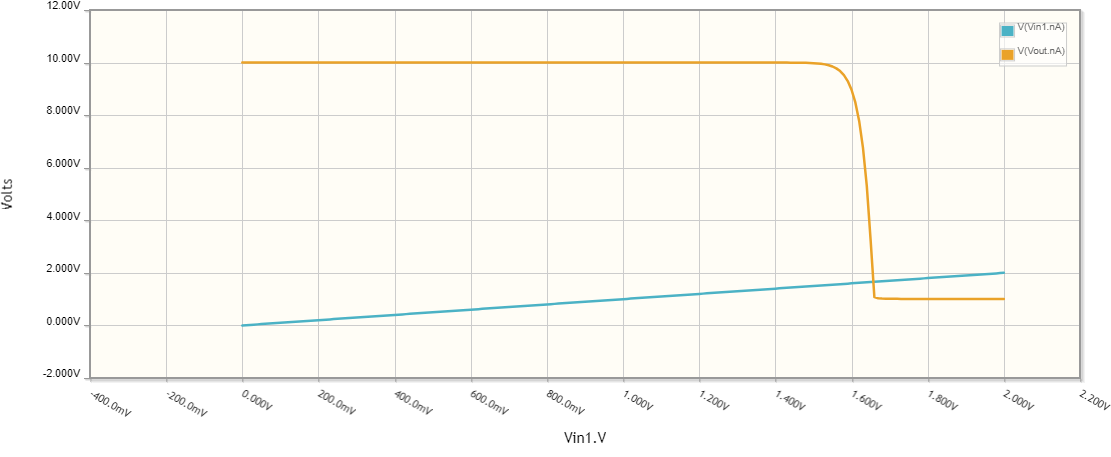
Vin2' = const (single-ended amplifier). The emitter is "immovable"...

simulate this circuit
... and the gain is maximum.

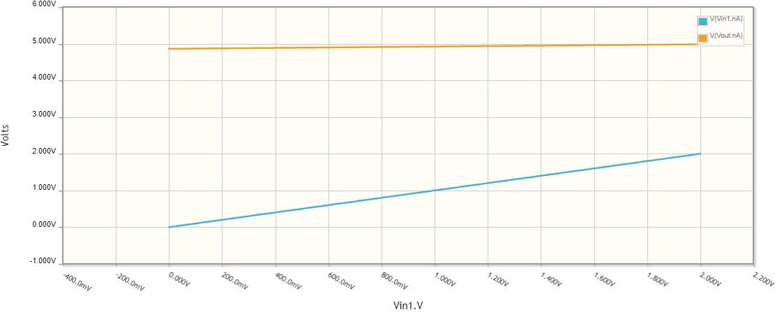
Vin2' = Vin1 (no amplifier). The emitter is "movable" (the behavioral voltage source Vin2' follows Vin1 with 0.642 V lower voltage)...

simulate this circuit
... and the gain is minimum.

In the practical circuit this means to connect a second transistor "in parallel" to the first by joining their emitters. Thus we come to the famous "long-tailed pair".

simulate this circuit
Conclusions
The main reasons for transistor differential amplifier stages to be biased by injecting a current into the emitters are:
The emitter voltage must be able to follow the common-mode input voltages when they vary widely.
The transistor inputs must not be shunted by bias circuits to have a high input resistance.
The base bias currents flow through the input voltage sources that must be able to pass the currents through themselves.

