0
\$\begingroup\$

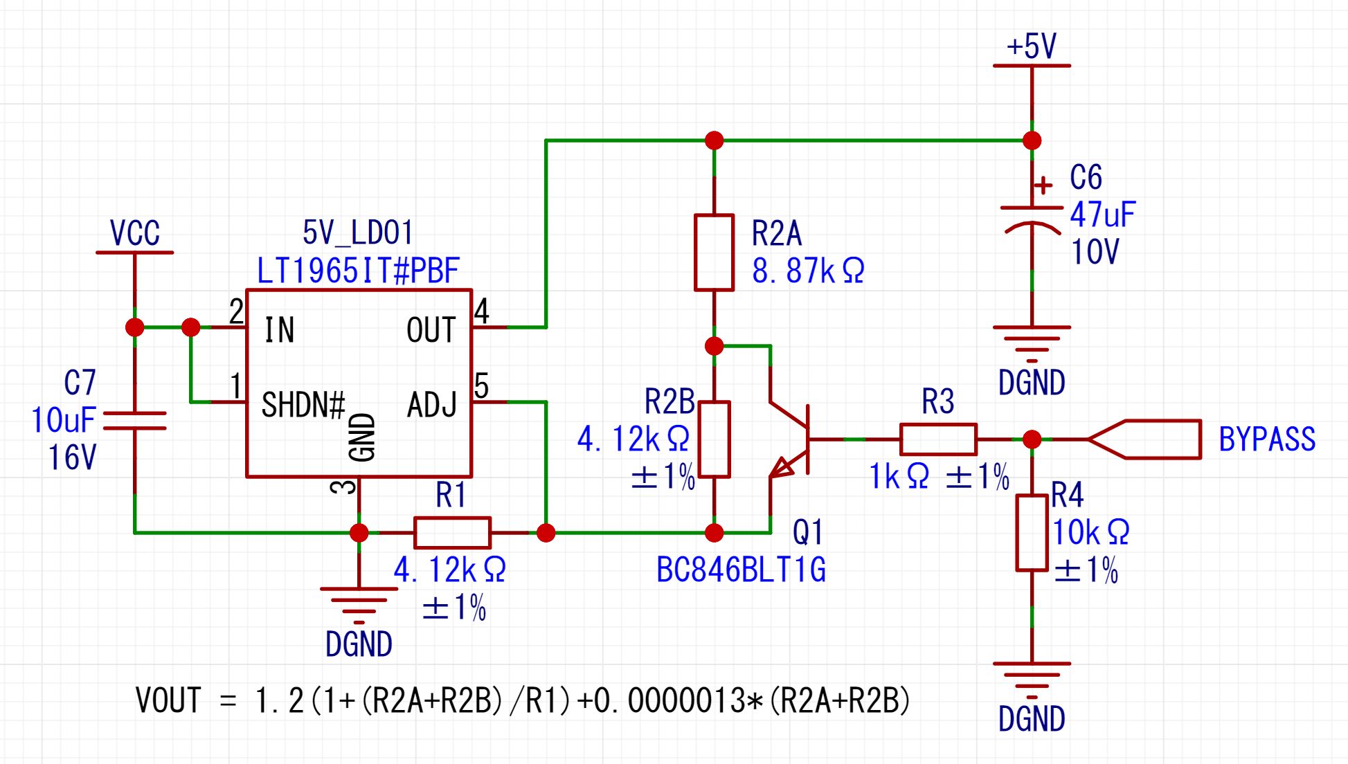
I'm designing an LDO power supply that is adjustable, I want to be able to switch between two output voltages using a MCU. I've designed the following circuit but can't test it as the parts are on order, do you think this circuit will work?

R1 and R2A+R2B form the feedback resistor divider for the LDO. The initial output voltage is set with both R2A and R2B values added up, and the output voltage is adjusted by turning on Q1 to short R2B.

LT1965 Transistor Adjustable

I've searched and could not find similar circuits.

LDO LT1965: https://www.analog.com/media/en/technical-documentation/data-sheets/1965fb.pdf

Thanks

\$\endgroup\$
2
  • 2
    \$\begingroup\$ If you are trying to short R2B why use a BJT instead of a MOSFET? I think you'll find that with a BJT the collector and emitter won't be at the same potential. \$\endgroup\$ Commented Feb 1 at 21:41
  • 2
    \$\begingroup\$ When you "short" R2B with the transistor Q1, there will still be some voltage across it, because BJTs never have a 0 Vce in saturation. You will have a more "ideal" "short" of R2B if you replace Q1 with a mosfet. \$\endgroup\$ Commented Feb 1 at 21:42

1 Answer 1

2
\$\begingroup\$

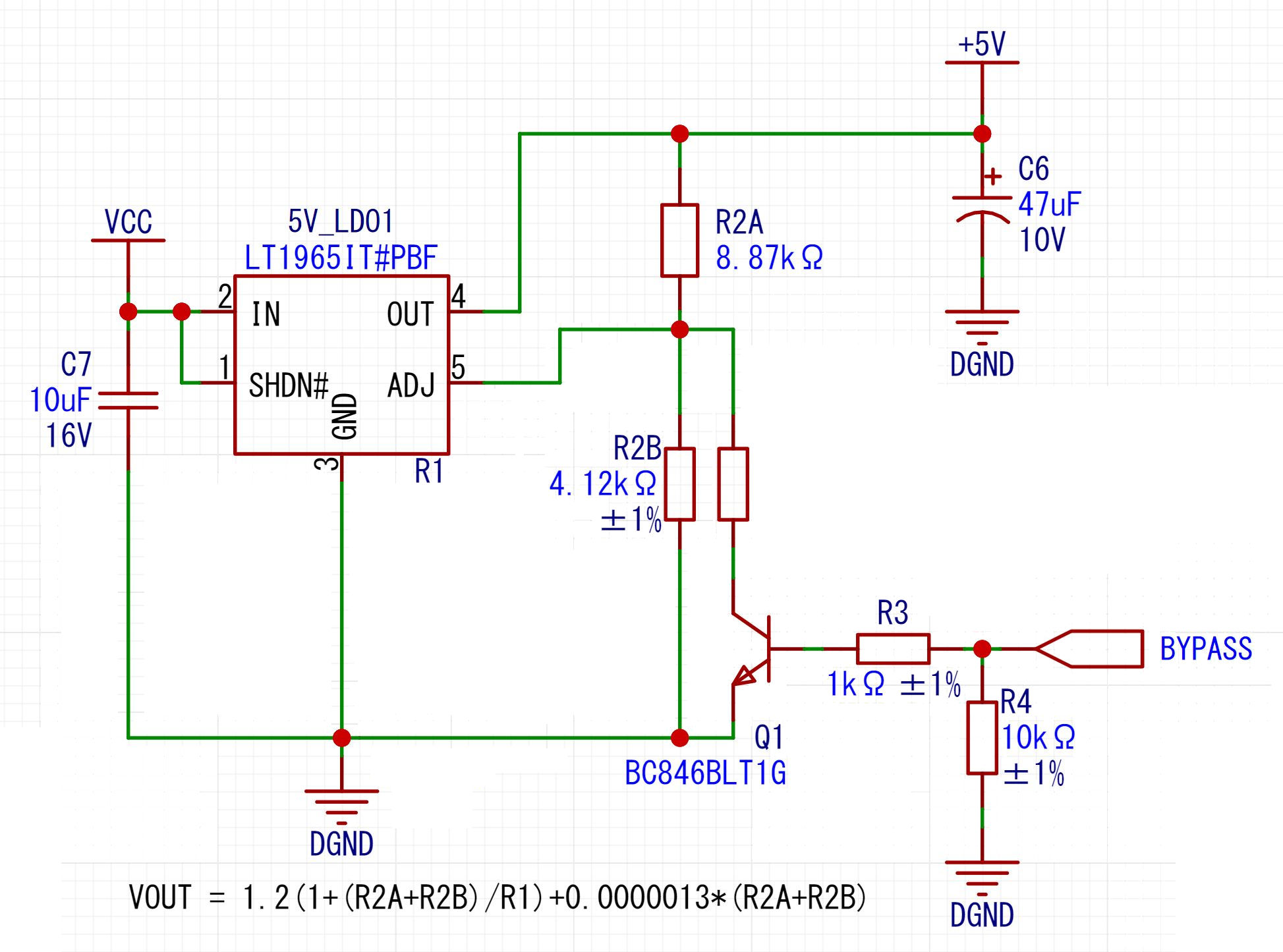
There are a few challenges in using a BJT as a switch in this way, one of which is that the base-emitter junction is basically a diode and the base current has to come out of the emitter alongside the collector current. A better configuration grounds the emitter instead so that this doesn't matter:

enter image description here

Obviously this means that the function of the BYPASS input is now inverted compared to the original design as the switched resistor is now in the bottom half of the divider.

As noted in the comments, a BJT doesn't produce a Vce of zero in saturation, although you could calculate the switched resistance to compensate for this to some degree as you know that the ADJ pin will sit around 1.2V for proper regulation.

Alternatively, replace Q1 with an N-channel MOSFET which can produce a lower Vds. Ensure that it will be turned on sufficiently at the value of Vgs you'll be using to produce a low enough Vds for your needs (i.e. don't just look at the threshold voltage which is typically defined for a drain current of 100uA).

\$\endgroup\$
1
  • \$\begingroup\$ If you want to get even spiffier, one could use an analog switch IC in place of Q1, allowing multiple voltages that could be selected by dio or even a communication bus (like spi/i2c). For a smooth range, it's even possible to use a DAC to slide the feedback voltage around... \$\endgroup\$ Commented Feb 2 at 13:35

Your Answer

By clicking “Post Your Answer”, you agree to our terms of service and acknowledge you have read our privacy policy.

Not the answer you're looking for? Browse other questions tagged or ask your own question.