12
\$\begingroup\$

I'm trying to implement a boost converter using TI's TPS55340.

After spinning up the design, I have found that the output ripple is almost 8x what I expected to see given my design parameters. First, let's get into the design, schematic and layout.

In short, my design parameters:

  • Input voltage: 11-13 V
  • Output Voltage: 16 V @ ~3 A (WEBENCH set to 2.91 A)

Plugging this into WEBENCH resulted in the following implementation (link to HTML):

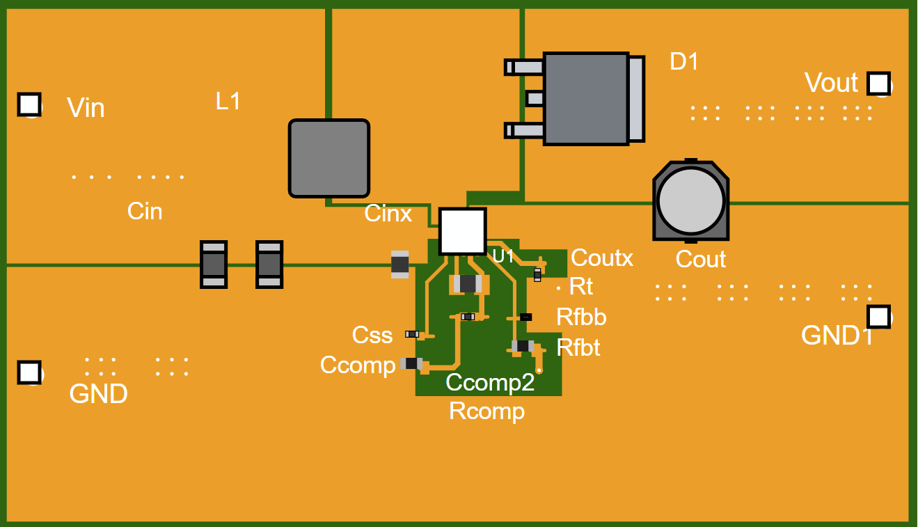
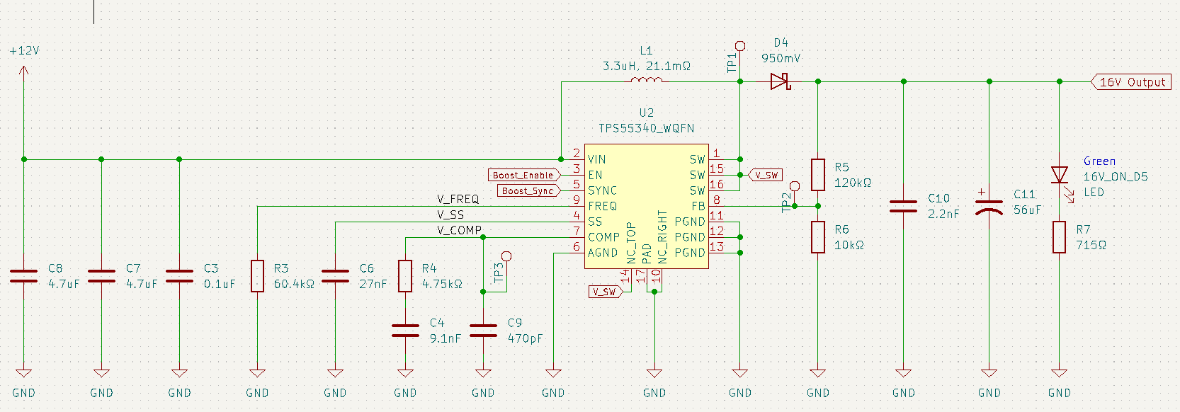
Schematic

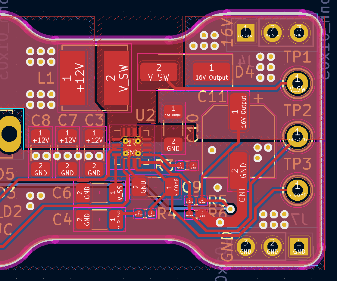
Layout

I translated this into KiCAD as follows:

enter image description here

And here's the region of my PCB where the boost converter is realized:

enter image description here

The input 12 V is input to the board less than 3 cm away via a DC barrel jack.

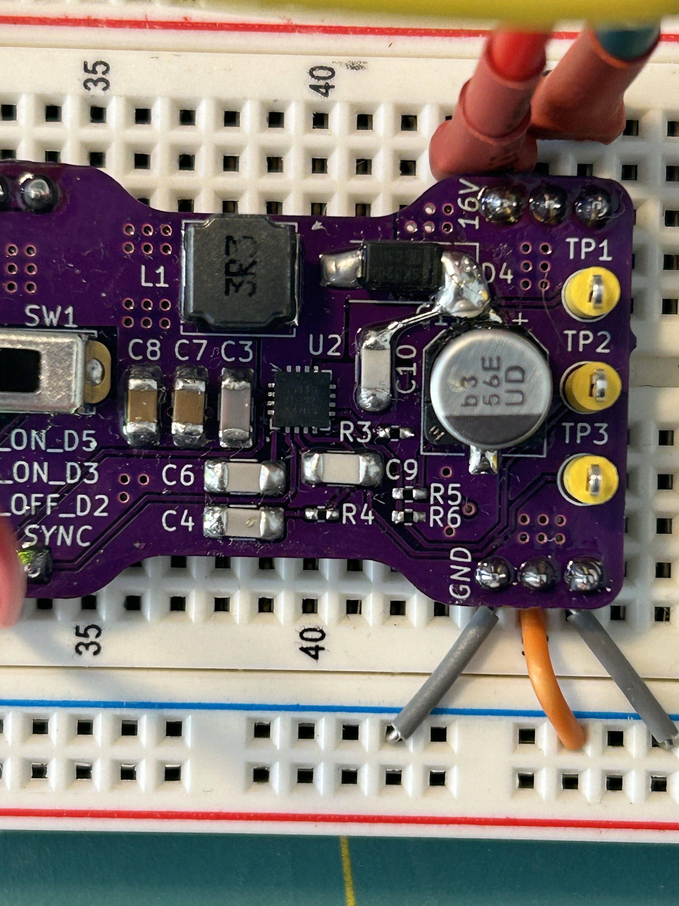
There is a mistake in the layout, I should not have sliced through the 16 V output plane with the V_SW test point, but I have fixed this with a few bodge wires. Here is a photo of the assembled region of the circuit:

enter image description here

You'll likely be interested in the critical components to implement the boost converter:

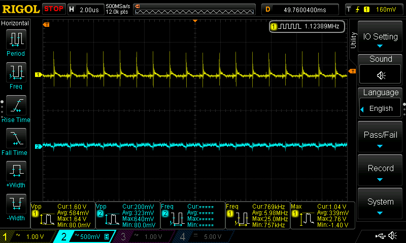
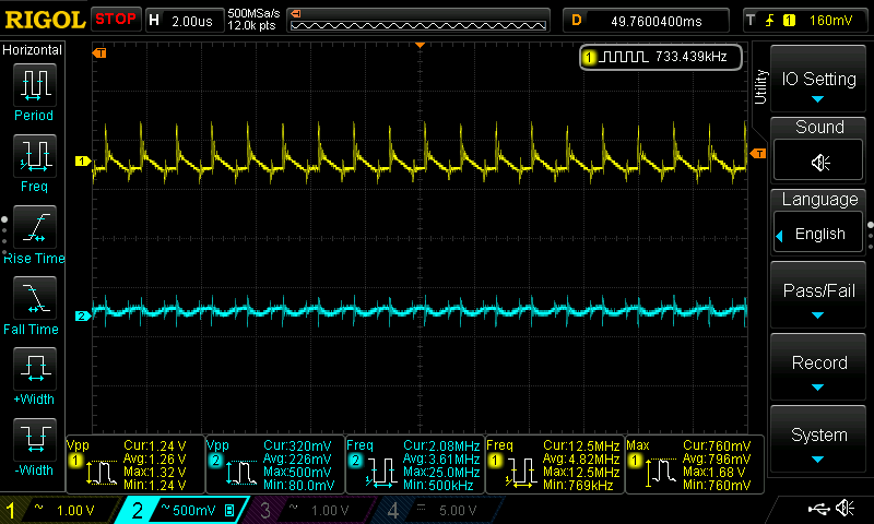
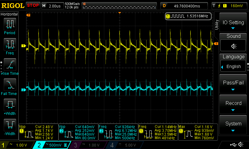
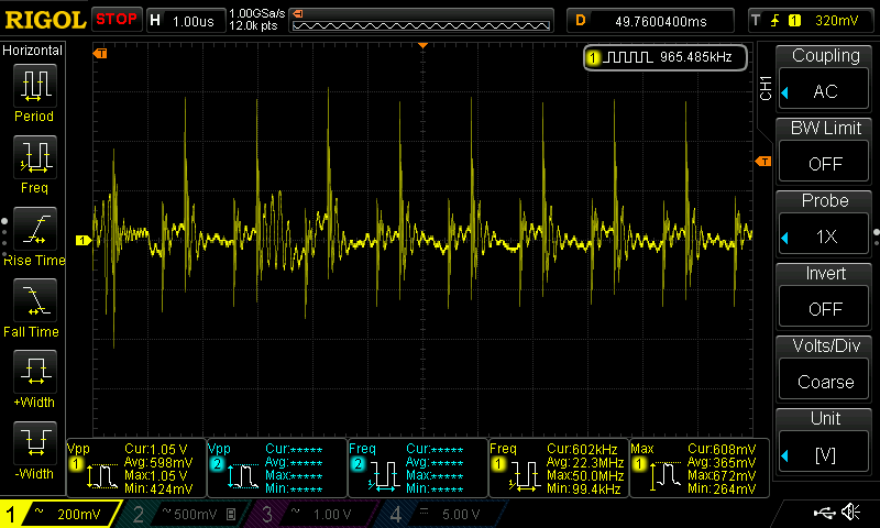
Using my benchtop power supply set to 12 V, and my DC load configured to draw 0.1 A, 0.5 A and 1 A, I measured the output using my oscilloscope and took screenshots. In each figure the 12 V input is the blue trace and the output is the yellow. Both channels are in AC coupling mode, and neither probe is using the ground alligator clip -- both are using the ring-tip ground spring.

0.1 A:

0.1A

0.5 A:

0.5A

1 A:

1A

The Vpp of the output being all the way up near 3 V is way out of spec for the design, according to the WEBENCH model it should be less than 57.5 mV.

I think the problem stems from a weak output diode. I notice that the part gets pretty hot during operation. What do you think?

If there is anything missing you'd like to see from the design, let me know.

Edit #1! Feedback has been incorporated, original design bodged:

The replacement parts have arrived and I've installed them on the PCB.

C11 is again 56uF but now has a much lower ESR. It's PN is 25SVPF56M.

C10 is now 1uF (up from 2.2nF). It's PN is
C1206C105K3RAC7800
.

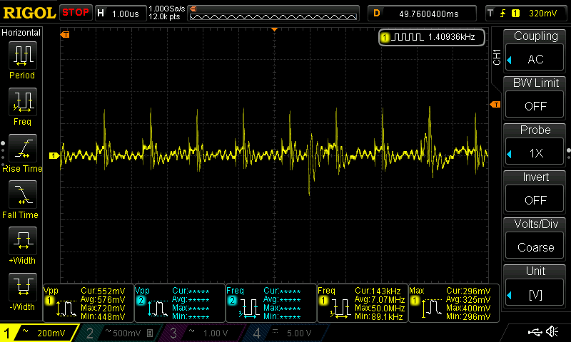
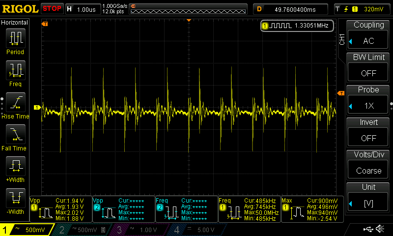
Here are the results. Same setup as last time, input power set to 12V, DC electronic load providing the load. This time we're only probing the output of the circuit.

0.1A:

0.1A, improved design

0.5A:

0.5A, improved design

1A:

1A, improved design

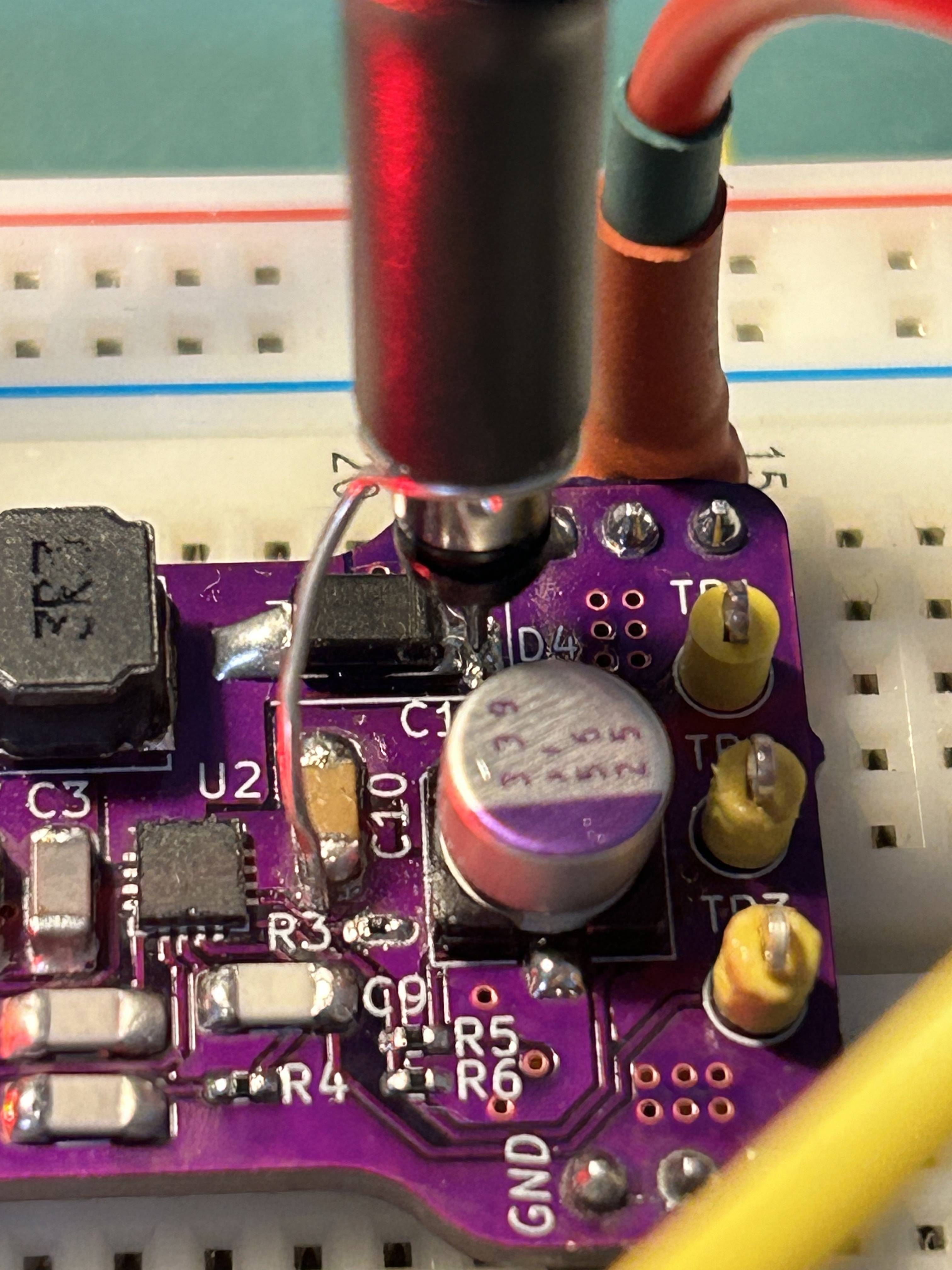
Here is the modified board (& probing setup):

Modified Circuit

The results here are mixed. At low current, the results are greatly improved. However, up at 1A there is still 2V of ripple on the output vs. the expected value of ~50mV.

This is likely due to the incorrect layout as pointed out by commenters.

Before I re-design the board to fix the errors, do these results point to additional problems with the design?

Edit #2! Design review of second revision:

Per the feedback from Jonathan S. and bobflux, I've come up with a second revision of this board and hope to submit it for more feedback prior to getting it manufactured.

In summary, the changes are as follows:

  • Removed large test points that sliced up the output pour.
  • Added a larger output diode that can handle more current.
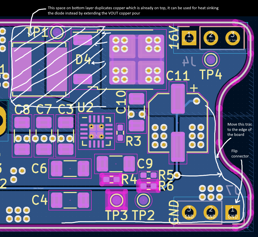
  • Added a copper pour below the output diode to remove heat.
  • Generally tightened output layout.
  • Add larger ground plane below the boost converter.
  • C10 is now 1uF.
  • C11 is a much lower ESR 56uF cap, 25SVPF56M.

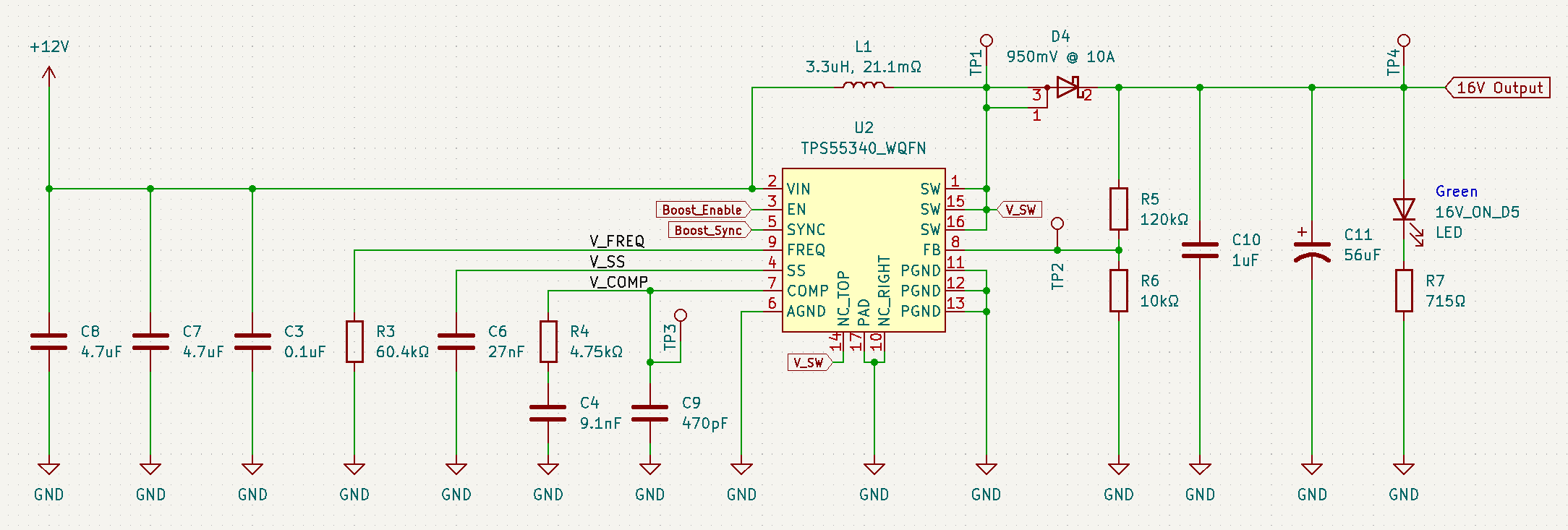
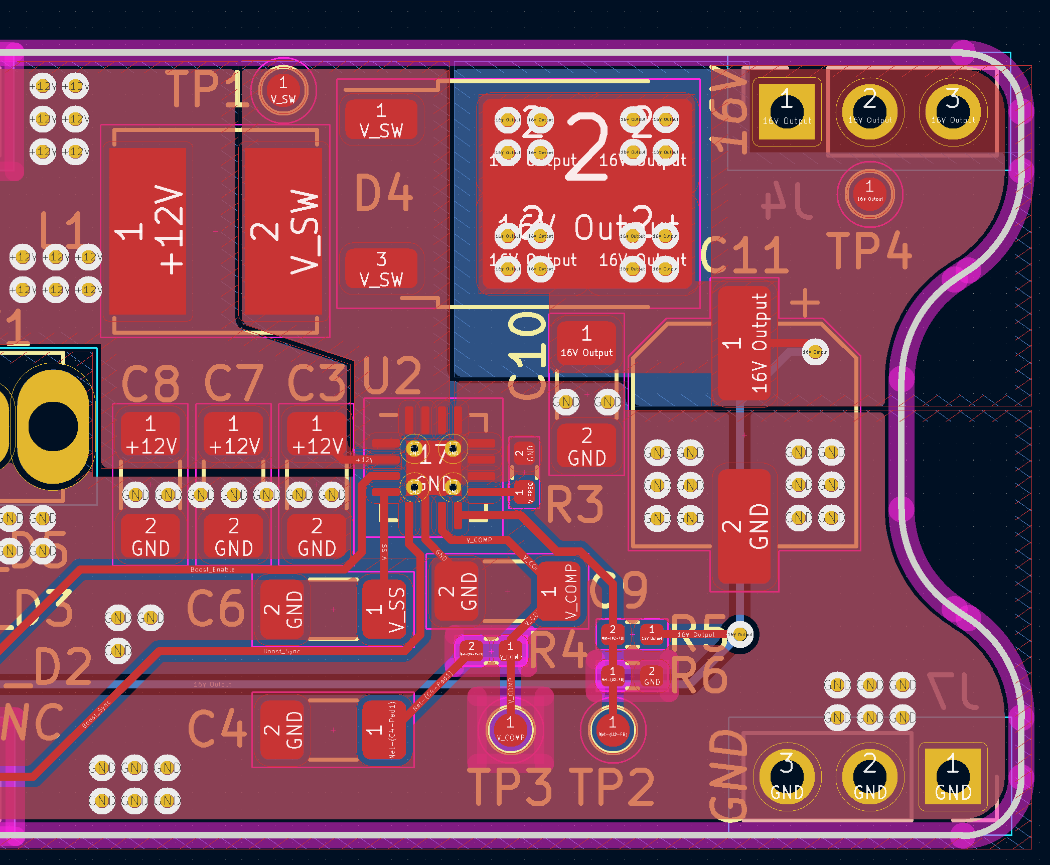
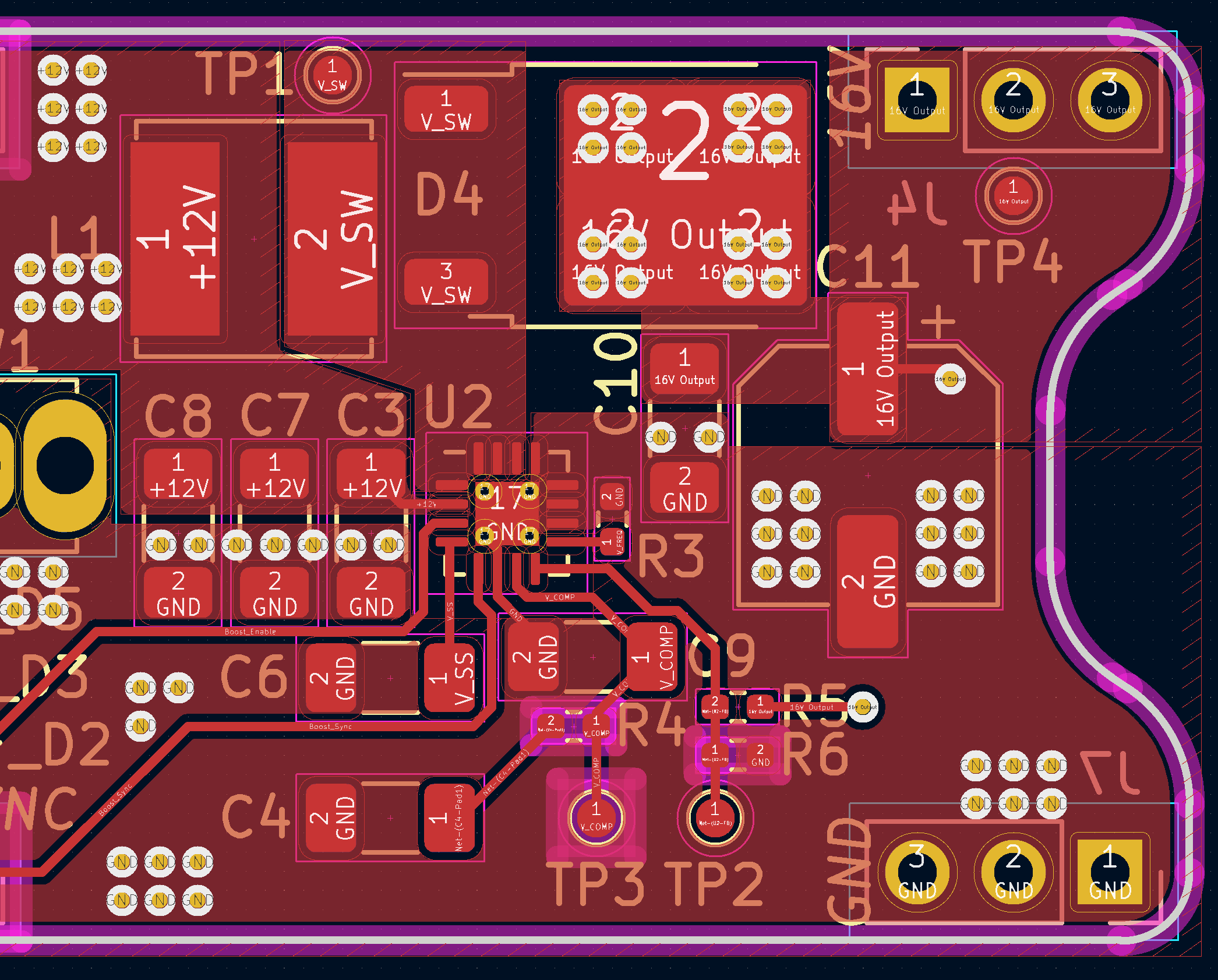
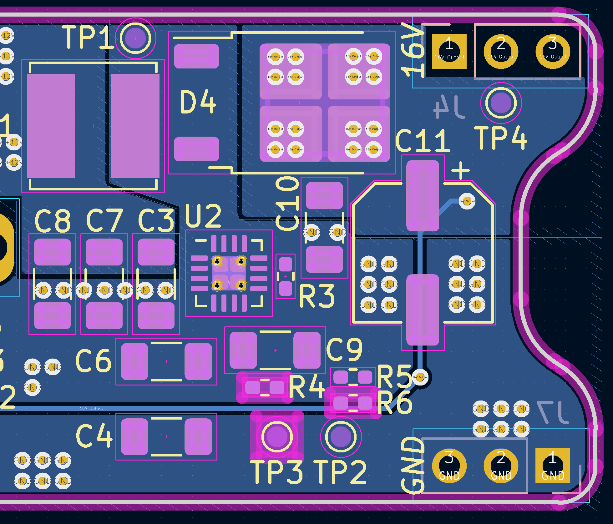
Here's the schematic:

Revision 2 Schematic

Here's the complete layout, followed by the front and back copper layers:

Revision 2 Layout Complete

Revision 2 Layout F Copper

Revision 2 Layout B Copper

I'll ask below for feedback, integrate it and then keep posting along with my progress.

\$\endgroup\$
3
  • \$\begingroup\$ Thanks to those that have pointed out that the problem is related to the output capacitance. I should have clarified. Configured WEBENCH to use an electrolytic on the output. This is because of the acoustic noise typically created by high value MLCCs. If anyone can point me to resources to mitigate this acoustic noise so I can use MLCCs that would be appreciated. \$\endgroup\$
    – esologic
    Commented Feb 18 at 18:07
  • \$\begingroup\$ Are you sure the electronic load is behaving well? An active load might respond strangely at these frequencies. Also if there's a long, wide, inductive loop between your module and the load, what you are seeing may not be entirely the module's fault. It's a long shot, but try to get a measure of performance under easy conditions, using a resistive load connected very close to the module output, before you start adding challenging loads. \$\endgroup\$ Commented Mar 8 at 4:44
  • \$\begingroup\$ This is a good point, the lead to the DC load is around half a meter in length. What would you suggest for a load circuit? Ideally I need it to consume 16V @ 1A, much more power than your standard 1/4W resistors could do. \$\endgroup\$
    – esologic
    Commented Mar 8 at 17:56

3 Answers 3

22
\$\begingroup\$

The diode is innocent. What you're seeing there is the effect of the output bulk capacitor's ESR (C11). According to the Digi-Key page you linked, its ESR is 0.44 Ohms. Given the waveform of the 1A trace, we can conclude that the converter is operating just at the edge of discontinuous conduction mode. The inductor ripple current should be about 2x the output current, which is 2A peak-to-peak in this operating mode. Multiplied with the output cap's ESR, you get an output ripple of about 1Vpp. This matches the triangular ripple waveform on the 1A oscilloscope trace.

The output bulk capacitor should ideally have 20mOhms ESR or less. Yours has almost 25x of that.

You simply chose the wrong capacitor. C11 needs to be an Al-poly type. The Panasonic 25SVPF56M would fit the existing footprint. If you want some more capacitance, the Nichicon RSA1E101MCN1GS might also be a good choice.

The very short, large voltage transients that are superimposed on the triangular ripple waveform point at a lack of high-frequency bypassing, which means that C10 is also wrong. It should have much larger capacitance, i.e. 1µF X7R.

\$\endgroup\$
4
  • 1
    \$\begingroup\$ Okay great I've ordered the two caps you suggested, and ordered a 1uF X7R to swap in for C10. Thank you, I'll report back. \$\endgroup\$
    – esologic
    Commented Feb 18 at 16:55
  • \$\begingroup\$ I ordered new components, installed them and repeated the experiments to mixed results. Any more thoughts before I proceed with a board redesign? \$\endgroup\$
    – esologic
    Commented Mar 8 at 2:52
  • \$\begingroup\$ @esologic The new capacitors appear to do their job well since the ripple (the low-frequency sawtooth wave) is gone. The 10MHz+ ringing is caused by inductance of the layout. Look at the loop from the input cap, through the inductor and diode, through the output cap, into ground, and then back into the ground terminal of the input cap. This is the main current loop, and if it's too physically large, it has a lot of inductance that causes the LC ringing that you observe. You need a really, really tight layout for a converter like this one. \$\endgroup\$ Commented Mar 8 at 20:30
  • \$\begingroup\$ I have integrated your feedback into a second revision posted as an edit to my post. Any thoughts before I order? \$\endgroup\$
    – esologic
    Commented Mar 15 at 1:53
16
\$\begingroup\$

It's the output cap. According the the datasheet, C11 has maximum ripple current of 230mA RMS and 0.44 ohms impedance at 100kHz, some of this impedance is capacitive but the rest is 30-40 mOhms ESR.

It should also have an inductance around 4nH due to its construction.

You would need a cap rated for the ripple current and with low ESR/inductance.

The Vpp of the output being all the way up near 3 V is way out of spec for the design

If your DC-DC chip switches 1A in 10ns, with an output cap having 4nH of inductance, that results in e=Ldi/dt=0.4V spikes. In your case the spikes are much higher, because the cut in the output copper pour increases the effective inductance of your cap.

The rest of the ripple is due to output cap ESR.

The output cap receives a much higher ripple current that it is rated for so it will heat up and this will shorten its life.

A quick fix would be to solder the highest value X7R cap that will fit on C10's footprint, unfortunately C10 has no close vias to the ground plane which increases its inductance.

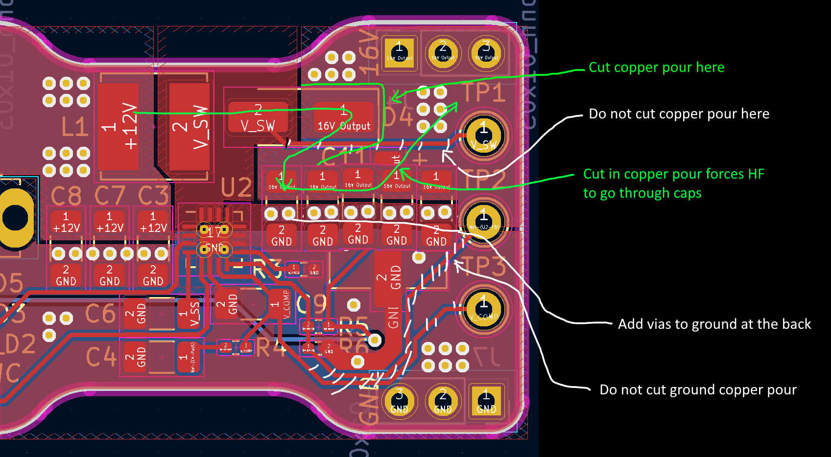
enter image description here

  • All the test points have to go. If you need them, put them on the back or anywhere else, but do not cut the copper pours: you need them to be whole for low inductance.

  • If possible, use all ceramic output caps. The usual 10µF MLCC has about 3 mOhms ESR, 1-2nH ESL depending on layout, and due to the extremely low ESR it can take a huge ripple current, ridiculous for its size. Using several in parallel means even lower ESR and ESL. In these low values the only electrolytic caps that could compete would be polymers, but... ceramics will simply be cheaper and have much lower inductance too.

In fact you can probably use the same MLCCs on the input and output, to get quantity discount.

If the chip does not like all-ceramic output caps, pick a chip that does.

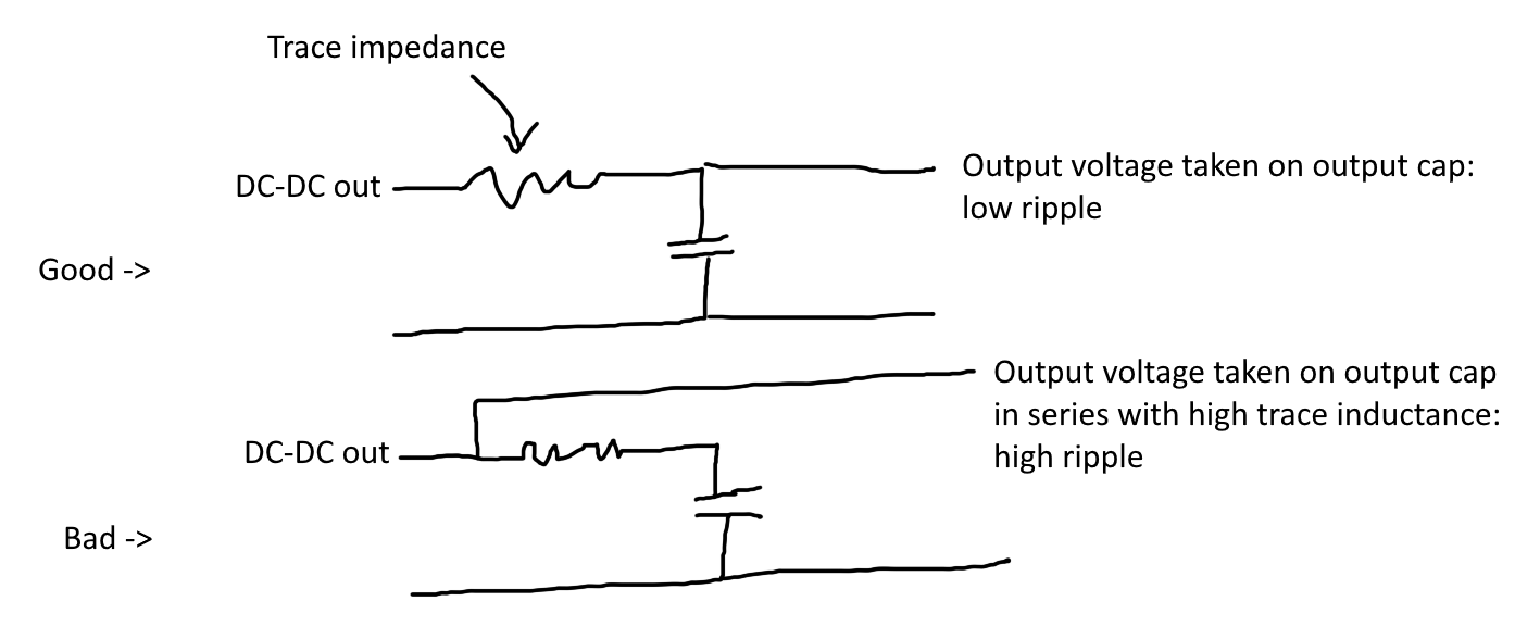
There is always some trace impedance in series with your caps. It's better if the output node is taken on the proper side of this impedance. That's why I added a cut (in green) in the output pour.

enter image description here

Regarding capacitor choice, 56µF 25V is an annoying value. The reason is a 10µF X7R 1206 MLCC only has a remaining capacitance of 3µF at 16V (see here, I used GRM31CR71E106MA12K). So if you use MLCCs only you need many, which takes up space. On the plus side, you get excellent ESR and ESL. So 56µF is too high for ceramics... but on the other hand, if you want to use an electrolytic cap, 56µF is too low because you'd get more low-ESR options with a higher value.

Note in the Webench simulation you linked, you can click on the parts and it will give you exact part numbers, which it also uses in the simulation. It recommends an OSCON polymer cap (same as Jonathan S quotes in his answer). Webench also takes into account inductor ESR.

I think the problem stems from a weak output diode. I notice that the part gets pretty hot during operation. What do you think?

Webench gives 2.76W diode loss, which is OK for the diode it recommends (it's a DPAK) but the much smaller diode you used will most likely overheat, the package is too small to conduct this amount of power into the PCB copper, and there is not enough copper to cool it. Also it's a lower current diode, so while it will have lower capacitance, thus lower switching losses in the MOSFET, its Vf at 3A is higher than the recommended diode, which increases conduction losses.

I see you made a very small PCB, so if you need it to be this tiny I would recommend a synchronous boost converter for the single reason of getting rid of the diode, and thus its dissipation, and thus the area required to cool it.


For the new version:

enter image description here

\$\endgroup\$
11
  • 3
    \$\begingroup\$ I hope it works! Yes MLCCs make noise, they behave both as piezoelectric microphones and loudspeakers: voltage ripple <-> vibration. Most DC-DC converters operate way above audio frequency so it's inaudible. What makes noise is the low-power mode when the chip periodically goes in and out of sleep to save power. It wakes up, pumps a few cycles to crank the output voltage up, then goes to sleep, leaving the output cap to power the load. This implies output voltage ripple. If it repeats at a frequency that is audible, then it will make a sound. \$\endgroup\$
    – bobflux
    Commented Feb 18 at 20:03
  • 3
    \$\begingroup\$ So if you want it to be silent, the key is to avoid audio frequency voltage ripple on your ceramic caps. If your load draws enough current so it never enters cycle-skipping or powersave mode, it'll be silent. But if you want to use the low power mode, then yes indeed you can use a larger electrolytic output cap. You still need MLCC in parallel for high frequency, but the large cap means the run/sleep cycles will be at a low frequency where your small PCB won't resonate. The inductor can also make noise. \$\endgroup\$
    – bobflux
    Commented Feb 18 at 20:07
  • 2
    \$\begingroup\$ OK I looked at the new scope shots: you're confusing ripple with HF spikes. Ripple is a sawtooth or sine wave at the switching frequency. With the new caps, it's almost gone, so good news. HF spikes are due to the layout issues: fast current switching (high di/dt) and L too high, which did not change. So I'd keep the OSCON, and replace the 1206 1µF MLCC with two 0805 MLCCs side by side like in my edited picture, plus other layotu advice in my answer like keep your polygons whole and remove all test points which were the source of the problem. \$\endgroup\$
    – bobflux
    Commented Mar 8 at 8:07
  • 1
    \$\begingroup\$ If you want a test point that uses almost no space and won't cause layout issues, you can use just a via, with a hole diameter wide enough to stick your scope probe in ; same for the ground spring. If possible you can move the output connector to where the old test points were: it will be closer to the output cap, which means less noise. Use as much copper as possible on the back for ground (the 12V polygon on the back doesn't seem to serve a purpose, it should be GND). You can post the new layout for a review. \$\endgroup\$
    – bobflux
    Commented Mar 8 at 8:16
  • 1
    \$\begingroup\$ Okay thank you again Bob. I'll work on the new layout and then post the new design for your review. \$\endgroup\$
    – esologic
    Commented Mar 8 at 17:54
5
\$\begingroup\$

If you look carefully at the Webench schematic, you'll see that you've ignored the specifications that were purposefully red-colored as being important :)

You also should show a photo of how exactly you probe your prototype. I bet you a bit of what we see is the resonance of the improper probing setup. You need to use very short, concentric probing tip that connects both the tip and the ground ring of the probe to the test points with <1cm of distance between the test point ground and probe tip ground ring. For this, the probe tip "grabber" must be removed, and ground clip cannot be used!

In the revised layout, you'll do well to provide test points specifically designed to accept the pin spacing of the high-frequency probing attachment on the scope probe. These accessories are typically provided with the probe.

I also don't see a continuous ground plane under the switcher.

\$\endgroup\$

Your Answer

By clicking “Post Your Answer”, you agree to our terms of service and acknowledge you have read our privacy policy.

Not the answer you're looking for? Browse other questions tagged or ask your own question.