0
\$\begingroup\$

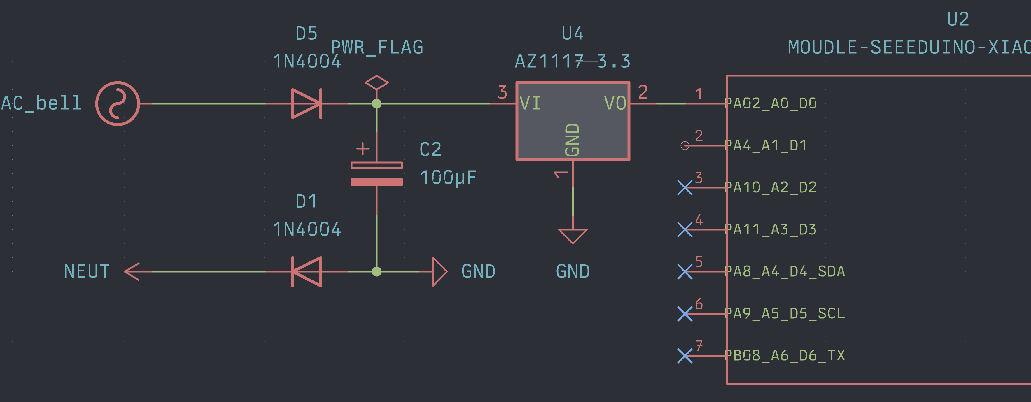
My project involves detecting a ringing doorbell. The doorbell circuit is 16 V AC and I want a low-voltage binary signal from it. The obvious way to me is to transform that electrical signal until its properties are useful (read: not harmful) to a digital GPIO. Firstly, by getting a DC signal by feeding it through a rectifier, secondly bringing it to my microcontroller's operating voltage with a voltage regulator. These ought to solve the AC and high voltage problems, but they don't cover current. A breadboard test showed 0.38 A from the regulator output, which I'd expect to be too much for a data GPIO.

Is this a real problem, or does the GPIO not actually need to sink all of that current?

If it is a real problem, what kind of circuit is needed to cut down that ~400 mA by a couple orders of magnitude?

Wiring diagram showing an incoming AC connected to a half-wave rectifier with a smoothing capacitor, connected then to a 3.3 V voltage regulator which sends its output to a GPIO pin on a Seeedstudio XIAO

\$\endgroup\$
8
  • 3
    \$\begingroup\$ The voltage regulator makes no sense. (The large C2 even less - why did you do that?) I'll assume you're familiar with basic circuits - why not simply use a plain voltage divider? \$\endgroup\$
    – sina bala
    Commented Feb 18 at 1:48
  • 2
    \$\begingroup\$ If there was 0.38A into a GPIO pin, the MCU should be damaged now. How did you measure it? Not with a multimeter in current mode, connected between regulator output and ground? \$\endgroup\$
    – Justme
    Commented Feb 18 at 2:06
  • 2
    \$\begingroup\$ Where did you measure the 0.38 A? Did you short the power supply? This feels very much like a basic (but common) misunderstanding about how power supplies (and electronics in general) work. Your voltage regulator will not forcibly "push" 0.38 A into your GPIO pin. Just use a simple (and safe) optocoupler circuit as described in the answers. \$\endgroup\$
    – StarCat
    Commented Feb 18 at 8:33
  • \$\begingroup\$ @sinabala I'm using a voltage regulator because 1) I have one, 2) don't need to bother calculating the resistor ratio, and 3) it's safer against voltage fluctuations from the input. As for the large resistor, again I used it because it's what I have on hand and seems to work fine \$\endgroup\$
    – Jonah
    Commented Feb 18 at 20:15
  • \$\begingroup\$ @Justme I did not connect it to the GPIO, I passed it through a multimeter as you described. Is that not the correct way? \$\endgroup\$
    – Jonah
    Commented Feb 18 at 20:16

5 Answers 5

2
\$\begingroup\$

You fail to describe the nature of the AC signal, other than its amplitude, and even that is ambiguous. Is that RMS or peak voltage? This source has two terminals, and all we know about it is that one of the "terminals" of that AC source rises and falls in potential with respect to the other, cycling between 16V higher in potential (or 23V if it's RMS), then 16V (or 23V) lower. We don't know the potential of either individual terminal with respect to the microcontroller's own ground, and without such knowledge it's foolish to connect either directly to your circuit.

I do not doubt this is why you have 0.38A flowing. You don't say where the 0.38A are flowing, but I suspect diode D1 is responsible, because of the unknown potential of the node you call "NEUT" with respect to ground.

When in doubt like this, the only safe solution is to galvanically isolate both terminals of the source of 16V AC from the rest of your circuit:
schematic

simulate this circuit – Schematic created using CircuitLab

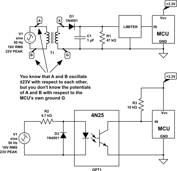
In the top circuit, I use transformer T1 as the isolating element. It will be bulky, heavy and expensive, and this method is not recommended. In this arrangement, T1 provides me with a "copy" of the potential difference V1, but also permits me to safely "ground" one side of that copy (node G), so that I can be sure that the other terminal (node X) is rising and falling in potential by ±23V with respect to that ground. Only then can I rectify it, with D1 and C1.

Your regulator AZ1117 would probably work as the "limiter" here, but it's not designed for this. It's a complex IC designed for a (relatively speaking) stable input potential, and which provides a stable, lower, output potential. Using it as a level translator here is not a good idea.

The lower circuit employs a 4N25 (or similar) opto-isolator (sometimes called opto-coupler), to galvanically isolate the 16V AC source from the MCU circuit. In this setup the 16V source is used to illuminate an LED, which switches on a transistor. We can safely connect that transistor to our MCU circuitry, bringing the "information" signal to our own ground level, without worrying what voltage shenanigans are happening on the AC side.

Diode D3 is needed to protect the LED, by ensuring that it can never be significantly reverse biased. Do not omit D3.

The above implementation will cause the MCU input to pulse once for every input AC cycle, which is probably not what you want. You can condition the pulses to become a steadier, prolonged "low" (0V) signal when input AC is present, but returning high (+3.3V) 0.1s or so after AC disappears:

schematic

simulate this circuit

\$\endgroup\$
2
  • \$\begingroup\$ Thank you for the diagrams and more importantly for explaining why galvanic isolation is important; I'd seen transformers in rectifier diagrams but didn't understand the purpose. I was also worried about the potential between the AC circuit and the ground of my microcontroller's power supply so understanding that isolation fixes that is super helpful. \$\endgroup\$
    – Jonah
    Commented Feb 18 at 20:31
  • \$\begingroup\$ Also you're totally right about my description of AC. I was using a multitester and just assumed that was reading peak (not knowing that RMS was even a thing). Good to know that the peak is greater than what I thought. \$\endgroup\$
    – Jonah
    Commented Feb 18 at 20:34
6
\$\begingroup\$

Several answers have mentioned optocouplers but they have not mentioned that there are AC input optocouplers that have back to back LEDs, for example this one.

With these the phototransistor is illuminated on both halves of the AC cycle, and it eliminates having to add an external diode or rectifying the AC voltage.

schematic

simulate this circuit – Schematic created using CircuitLab

\$\endgroup\$
4
  • \$\begingroup\$ Oo that's perfect, that would really simplify the whole thing, thank you! Same question, I see your circuit diagram converts the incoming voltage into a low signal instead of a high signal and I'd like to understand the reasoning behind that. \$\endgroup\$
    – Jonah
    Commented Feb 18 at 20:44
  • 1
    \$\begingroup\$ @Jonah The output is from an NPN transistor, so we use a common emitter configuration to pull the collector low. That works better than trying to pull the emitter high with common collector which would put the load in the transistor’s input circuit. You might find a different opto with a PNP or FET that would be better for an active high output but NPN is much more common and it’s easier to just invert the logic in software if necessary. \$\endgroup\$
    – GodJihyo
    Commented Feb 18 at 21:04
  • \$\begingroup\$ Could I avoid needing an external resistor if I use the pin in PULLUP mode, and use the transistor to pull the pin low? \$\endgroup\$
    – Jonah
    Commented Feb 19 at 4:29
  • 1
    \$\begingroup\$ @Jonah I think that should work. \$\endgroup\$
    – GodJihyo
    Commented Feb 19 at 4:54
3
\$\begingroup\$

Safest way is to use an optoisolator. Here is a method, showing the response time to a brief buzz of the bell.

enter image description here

The 4 diodes can be a packaged bridge rectifier of just about any kind with an adequate voltage rating.

\$\endgroup\$
2
  • \$\begingroup\$ This seems relatively straightforward, your diagram shows the AC still being rectified, but then isolated with an octocoupler instead of trying to drop the voltage/current as I was pursuing. I see that you're converting the input AC into a low signal, I'm interested in understanding why you'd do it that way around instead of converting it to a high signal? \$\endgroup\$
    – Jonah
    Commented Feb 18 at 20:40
  • 1
    \$\begingroup\$ It's pretty arbitrary whether you choose to swap the opto transistor and 47kΩ resistor or not. There may be some slight advantage to the way I've shown it in that you can perhaps use an on-chip pullup and lose the resistor or that noise capacitively coupled through the opto is returned to ground rather than Vdd. Active low inputs are perhaps more common than active high for historical and other reasons. \$\endgroup\$ Commented Feb 18 at 21:23
2
\$\begingroup\$

Your circuit makes a very little sense.

One solid/safe way is to use a standard optocoupler (like old 4N25X or VO615A, page4 )

enter image description here

A 10k series resistor and extra diode on input (in parallel, in opposite direction) will do the job.

\$\endgroup\$
0
1
\$\begingroup\$

Thanks to the many helpful answers, I've learned a lot about the properties of this problem space. It seems like my main problem is that even if I found a "neutral" pole on the incoming AC, I couldn't trust its potential relative to my circuit's GND, which would absolutely fry my components. Because of this, galvanic isolation is needed so to acquire a voltage relative to the device ground. All of the answers suggested an optocoupler because of their size, cheapness, and ease of integration here by pulling the GPIO low.

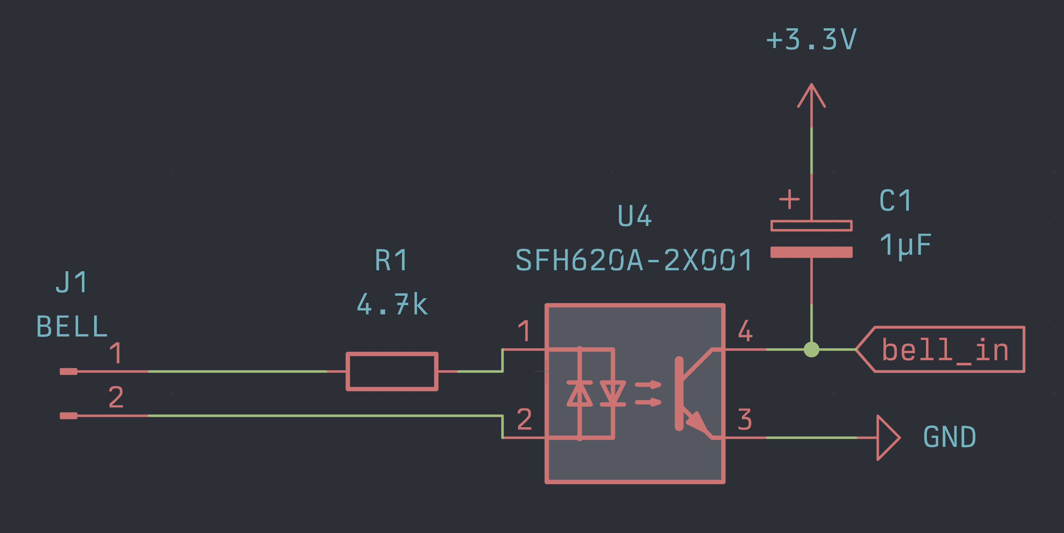
Here is my revised design. It uses a small capacitor on the output as @Simon Fitch suggested to prevent cut-off at the cycle midpoint, and an AC input optocoupler as @GodJihyo suggested to remove the need for a rectifying diode. This schematic assumes the MCU GPIO (bell_in) has an internal pull-up resistor.

The AC bell circuit connected to a SFH620A optocoupler through a 4.7k resistor in series; the collector of the optocoupler is connected to 3.3v via a 1uF capacitor and to the bell_in net, and the emitter tied to ground

\$\endgroup\$
4
  • 1
    \$\begingroup\$ Signal processing (signal latching and/or integration etc.) can be done easily in software, it is cheaper than the cap. \$\endgroup\$ Commented Feb 19 at 6:35
  • \$\begingroup\$ You're probably right but I didn't think that would work if I want to use it as a sleep interrupt signal \$\endgroup\$
    – Jonah
    Commented Feb 19 at 23:05
  • \$\begingroup\$ For an interrupt it is exactly what you need - only a single pulse will do the job. Why would you need a constant level out of this? \$\endgroup\$ Commented Feb 20 at 1:43
  • \$\begingroup\$ What I need is a single edge of any kind. Without a capacitor I'm going to get an interrupt every 1/60th of a second while the doorbell is pressed which is more interrupts than I need (unless you're implicitly suggesting that the first interrupt should instruct the MCU to deregister the interrupt). Regardless I plan to test it's behavior without. I'm not certain that it's needed, but it is better to have a PCB with a room for that component than to found out I need it later. Simply not installing it would have the same effect as never designing for it in the first place. \$\endgroup\$
    – Jonah
    Commented Feb 20 at 6:08

Your Answer

By clicking “Post Your Answer”, you agree to our terms of service and acknowledge you have read our privacy policy.

Not the answer you're looking for? Browse other questions tagged or ask your own question.