The inputs of the power amplifier are biased internally, to +3V (wrt. the IC's GND), which is detailed on page 3 of the datasheet. The solution is not to add your own biasing after C1, which would mess up the DC conditions established by the TPA3137 itself, but rather to constrain the output of whatever stage comes before it.
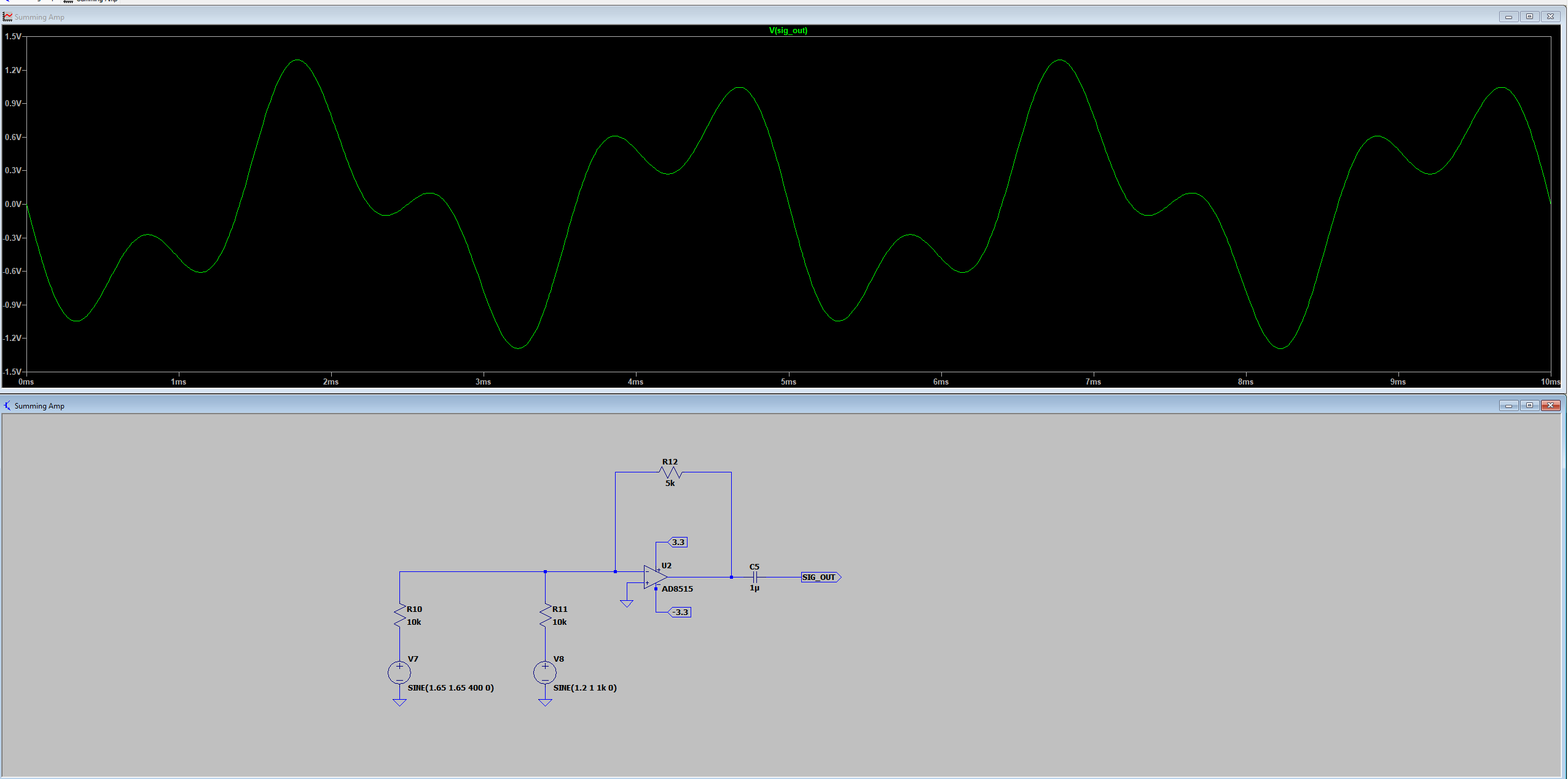
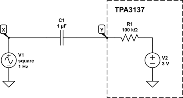
Start by considering what can happen if your summing amplifier outputs a square wave going between +3.3V and -3.3V, which it could conceivably do:

simulate this circuit – Schematic created using CircuitLab
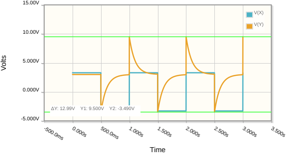
I don't know if 100kΩ is the actual input resistance, this is a qualitative illustration only. Here's a plot of the summing amplifier output potential \$V_X\$ and the resulting \$V_Y\$:

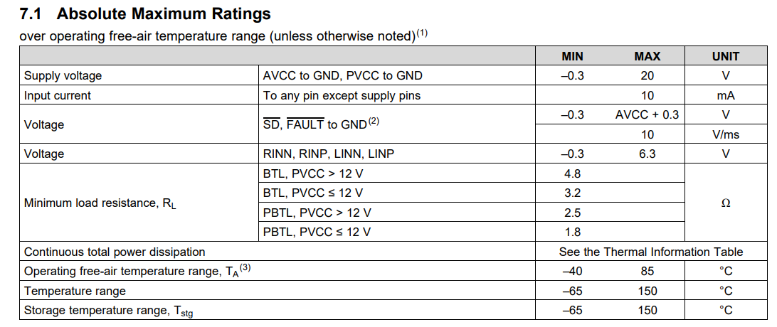
As you can see, your problem is not only on the negative parts of the signals, but positive also. Both possible extremes of -3.5V and +9.5V can damage the TPA3137.
Clearly the differentiator formed by C1 and the TPA3137's input resistance is (under certain conditions) able to produce amplitudes two times the amplitude of the signal at X. That's 12V peak-to-peak for a square input of 6V peak-to-peak. The largest acceptable swing at Y is a little over 6V peak-to-peak; about \$+3V \pm 3.3V\$.
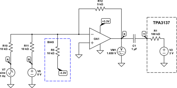
Therefore, the largest signal amplitude that your summing stage should produce is a little over 3V peak-to-peak. Considering that C1 is blocking DC, this could be, say, 0V and +3.3V, which means that a (rail-to-rail output) op-amp with supplies of 0V and +3.3V would work fine to apply that constraint.
However, you would also have to bias the summing op-amp half way, at +1.65V or so. That's easy to do:

simulate this circuit
Note: Don't use the power supply to offset the output, like I do here, because any supply noise will be injected directly into the signal. Rather use a precision reference, such as a TL431, or some other low-noise source, and you should definitely low-pass filter that source.
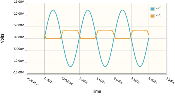
The blue box is simply adding 1.65V DC offset to the output. Even with a grossly over-sized input from one of the sources V7 or V8, the op-amp's output will be clipped to stay safe. Here's \$V_A\$ (blue) and the resulting \$V_X\$ (orange):

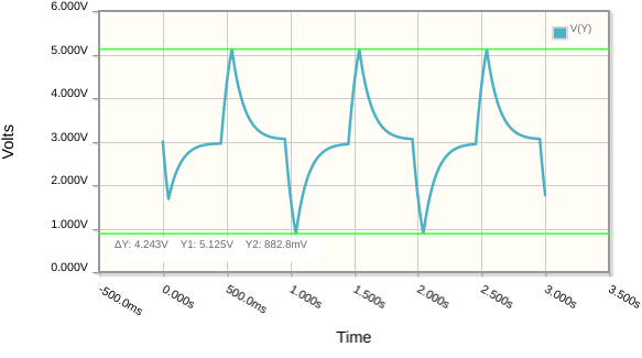
The corresponding TPA3137 input, \$V_Y\$:

If you absolutely have to use a bipolar supply for your op-amps, or even a supply greater than ±3.3V, (perhaps because they're all in the same package and some of them require such a supply, or they're not rail-to-rail output), then you'll need to constrain the output in some other way.
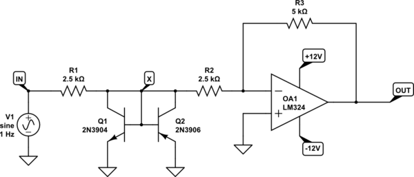
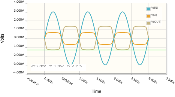
This could be as simple as reducing gain so that no possible input combination could ever produce an output amplitude greater than 3V peak-to-peak, or you could clamp the inputs. Here I use diode-connected transistors:

simulate this circuit
Those transistors pass no current when the potential at X lies between +0.7V and -0.7V, but they become very conductive otherwise. This effectively prevents X from ever leaving that range, constraining the output to about ±1.4V:

Whichever solution you employ, the goal will always be to prevent the output of whatever is driving C1 from ever significantly exceeding 3V peak-to-peak.

