0
\$\begingroup\$

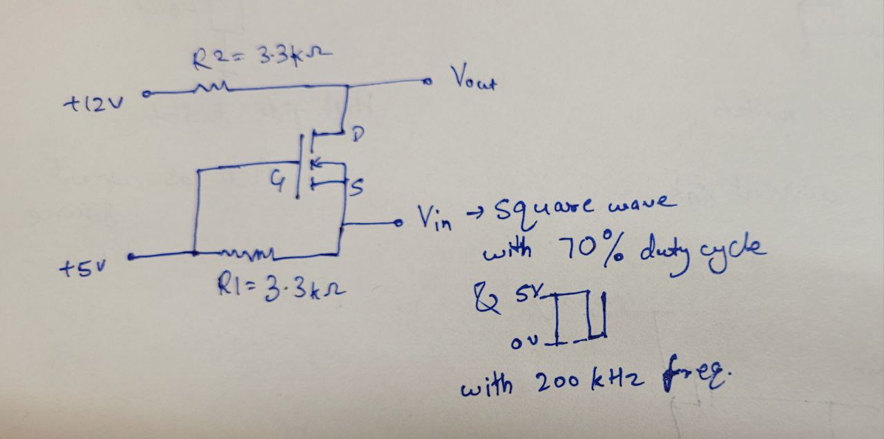
I want to translate +5V HIGH, 0V LOW logic from Arduino Uno to +12V HIGH, 0.5V LOW logic using IRF540N enhancement type n-channel MOSFET. The circuit I have referred is from https://circuitdigest.com/tutorial/bi-directional-logic-level-controller-using-mosfet and the circuit is

IRF470N circuit for level translation

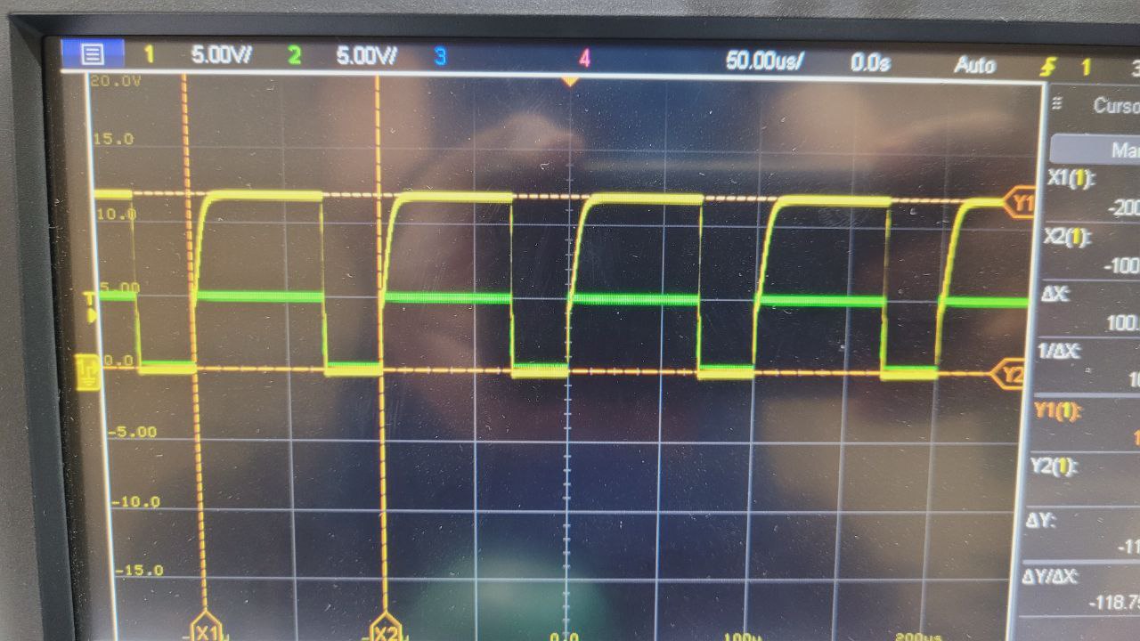
At the input Vin, I'm providing a square wave at 70% duty cycle with +5V HIGH & 0V LOW. Initially I was driving the circuit at 10 kHz and was able to get a beautiful waveform.

10kHz output

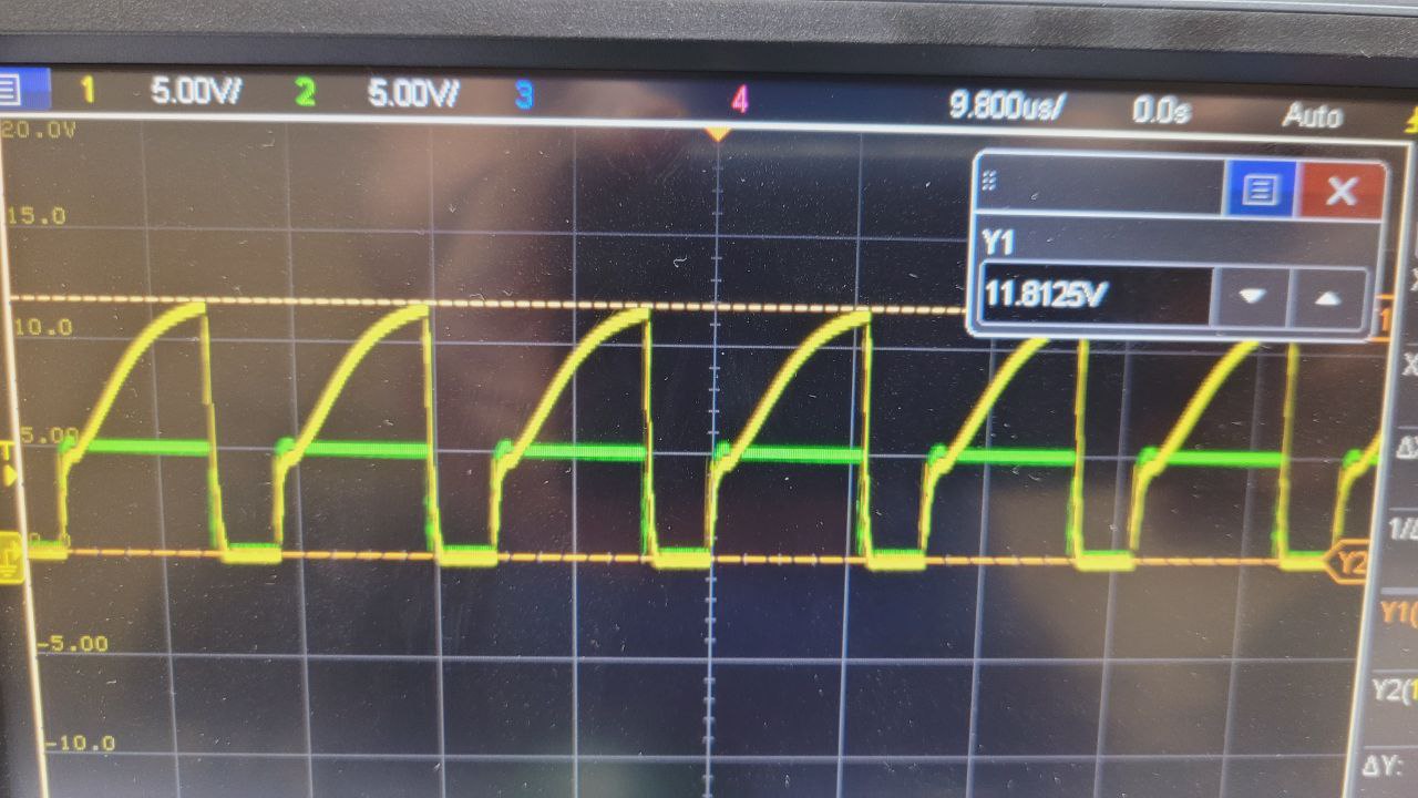
But as I was increasing the frequency up to 200 kHz, the waveform is not a square wave anymore. Output at 65kHz:

65kHz output

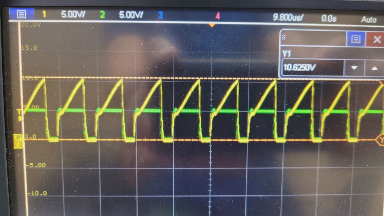
Output at 100kHz:

100kHz output

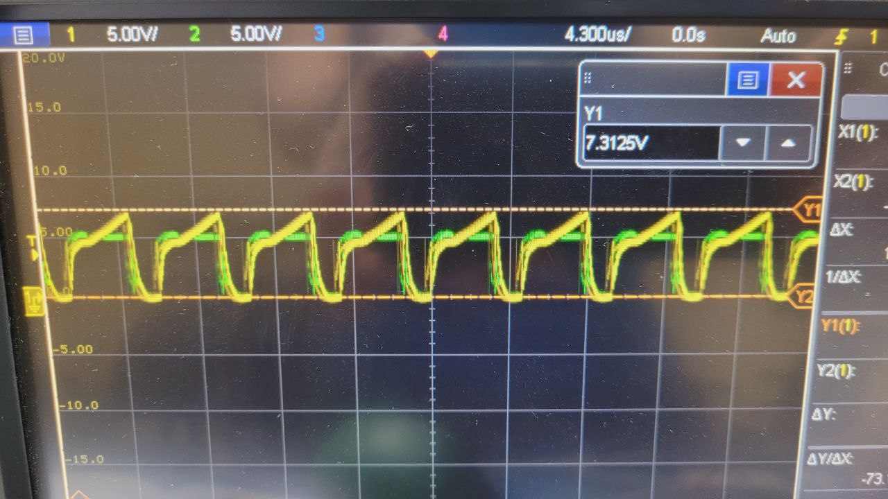
Output at 200kHz with peak voltage at 7.3125V:

200kHz output

I had chosen IRF540N considering the switching characteristics with 100 ns turn On time and 145 ns turn Off time as the at 200 kHz with 70% duty, it will 3500 ns HIGH and 1500 ns LOW but unable to get the desired output.

IRF540N switching characteristics

Someone please explain why this is happening even though the MOSFET turn on time is quite within the limits of switching time. Moreover is it possible to achieve +0.5V LOW logic level after translation with this circuit?

\$\endgroup\$
7
  • \$\begingroup\$ Is there a particular reason you want the translation range from 12V to 0.5V instead of 12V to 0V? \$\endgroup\$
    – MOSFET
    Commented Mar 26 at 16:02
  • \$\begingroup\$ As noted in the answer the gate charge is an issue. The IRF540N is a designed for switching 33 A and has a typical input capacitance of 1960 pF. Since this is for a level translation, perhaps a lower current device such as a LND150 N-Channel Depletion-Mode DMOS FET with a reduced input capacitance of 7.5 pF (typical) would give faster edges. Posting a comment as haven't tried simulating it. \$\endgroup\$ Commented Mar 26 at 16:14
  • \$\begingroup\$ @MOSFET basically it is driving a sensor which requires 12V to 0.5V logic clock to drive the digital elements \$\endgroup\$
    – Technaut
    Commented Mar 26 at 17:09
  • \$\begingroup\$ @Technaut your MOSFET selection is super over-kill for your application; I was anticipating a high-current load on the output. Post the sensor that needs that clock input spec. What I presented is a high-power level translator. \$\endgroup\$
    – MOSFET
    Commented Mar 26 at 17:14
  • \$\begingroup\$ Thanks @MOSFET for highlighting it. Initially I was planning to use FDT439N but due to unavailability, I thought of using IRF540N. Can you please suggest if FDT439N would be best suited for my application as I don't want to high-current to drive my sensor. Moreover little bit out of context from this question, I tried using TL074 opamp for this application but it has a slew rate of 20V/us. But then I realised an opamp with slew rate >240V/us would be a good match. Is it possible to comment on this? \$\endgroup\$
    – Technaut
    Commented Mar 26 at 17:44

2 Answers 2

0
\$\begingroup\$

It's not the gate charge capacitance; it's the drain source capacitance that is the issue. It forms a low pass filter with the 3k3 resistor that ties the drain to 12 volts. From the data sheet for the IRF540N, \$C_{OSS}\$ is 295 pF so, you form a low-pass filter with the 3k3 at a frequency of 163 kHz.

If you just want to try a different method, use an FOD8343 with the added bonus that it's isolated: -

enter image description here

Output rise and fall times are less than 40 ns. There are many other types of driver like this as well. I chose this for no other reason that I'd been using it in a design.

\$\endgroup\$
5
  • \$\begingroup\$ Isn't it due to both reasons, inadequate current for gate drive and drain source capacitance? I'm not very sound with MOSFETs, please correct me if it's not the case \$\endgroup\$
    – Technaut
    Commented Mar 26 at 18:42
  • \$\begingroup\$ It's mainly the drain-source capacitance. Look at your images and, look at the yellow waveform (your input). It remains pretty reasonable all the way through. Sure at 200 kHz it's starting to suffer a little but, compared to the output node there's no contest. Given that the gate is held at a fixed DC voltage (5 volts), providing the source drive signal is "strong" then the main problem is drain-source capacitance @Technaut \$\endgroup\$
    – Andy aka
    Commented Mar 26 at 18:50
  • \$\begingroup\$ So if I use 1k resistor (R2 in my diagram) instead of 3k3 resistor, it will form 539 kHz low pass filter and that will suffice the requirement. Will this work? The resistor was used as pull-up if I'm not wrong \$\endgroup\$
    – Technaut
    Commented Mar 26 at 19:04
  • \$\begingroup\$ @Technaut Is the square wave at the source capable of pulling low with 12 mA flowing through the MOSFET? This is why I have suggested a different approach in my answer because, if you are not careful, you will transform a problem in one area to a problem in another. If we are done here, please take note of this: What should I do when someone answers my question. If you are still confused about something then leave a comment to request further clarification. \$\endgroup\$
    – Andy aka
    Commented Mar 26 at 19:17
  • \$\begingroup\$ It worked with 1k resistor (R2). I'm getting an output similar to the 65 kHZ output which I have posted in the question. It is not a clean square wave but i think it will work fine. Thanks! \$\endgroup\$
    – Technaut
    Commented Mar 27 at 5:17
1
\$\begingroup\$

You don't gave enough current to drive the gate; you are current-limited and you are going to need a proper driver for high-speed switching. The fundamental issue is the gate charge (capacitance) that has to be overcome and can't be realized with a passive circuit like this.

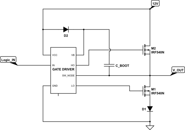
What you really want is a half-bridge driver for high-speed switching. Here's what I would do to convert 0V-5V logic to 0.5V-12V level-shift:

schematic

simulate this circuit – Schematic created using CircuitLab

Some gate drivers will have the diode integrated into the IC for simplicity.

\$\endgroup\$
4
  • \$\begingroup\$ Thanks for the circuit simulation link but I'm unable to simulate it on CiruitLab. It's showing "Solve Aborted - Error in Transient Solver". I tried referring the documentation but unable to figure out the problem. I have provided it with a 200kHz clock at "Logic_IN" label, +12V supply at "12V" label, C_BOOT with 0.1uf with DC sweep from 0 to 10us with 10ns time-step. Can you please help with this. \$\endgroup\$
    – Technaut
    Commented Mar 26 at 18:36
  • \$\begingroup\$ @Technaut. The circuit I posted was for demonstration only; it was never intended to be simulated. But based on your description, this circuit is overkill for what you really need - This circuit is 1 inductor away from being an unregulated synchronous buck convertor. Your original circuit will work fine if you uses a smaller FET. What is the part number of the sensor? Your clock signal doesn't have to be perfect, likely "good enough" will suffice. \$\endgroup\$
    – MOSFET
    Commented Mar 26 at 19:27
  • \$\begingroup\$ I have come across this sensor SD3101 and was working out to deduce its driving circuit as it seemed quite challenging to me. \$\endgroup\$
    – Technaut
    Commented Mar 27 at 5:21
  • \$\begingroup\$ @Technaut The datasheet is kind of crappy so I could see this being challenging. I was hoping for better information on clock requirements, but what I've gathered: it's 25pF per pin (seems like there are 2 clock pins) with a rise and fall time of 8ns. Similar to what Andy suggested, I would use this: ti.com/lit/ds/symlink/ucc27614.pdf?ts=1711519222744 same principle, but faster. \$\endgroup\$
    – MOSFET
    Commented Mar 27 at 6:06

Your Answer

By clicking “Post Your Answer”, you agree to our terms of service and acknowledge you have read our privacy policy.

Not the answer you're looking for? Browse other questions tagged or ask your own question.