2
\$\begingroup\$

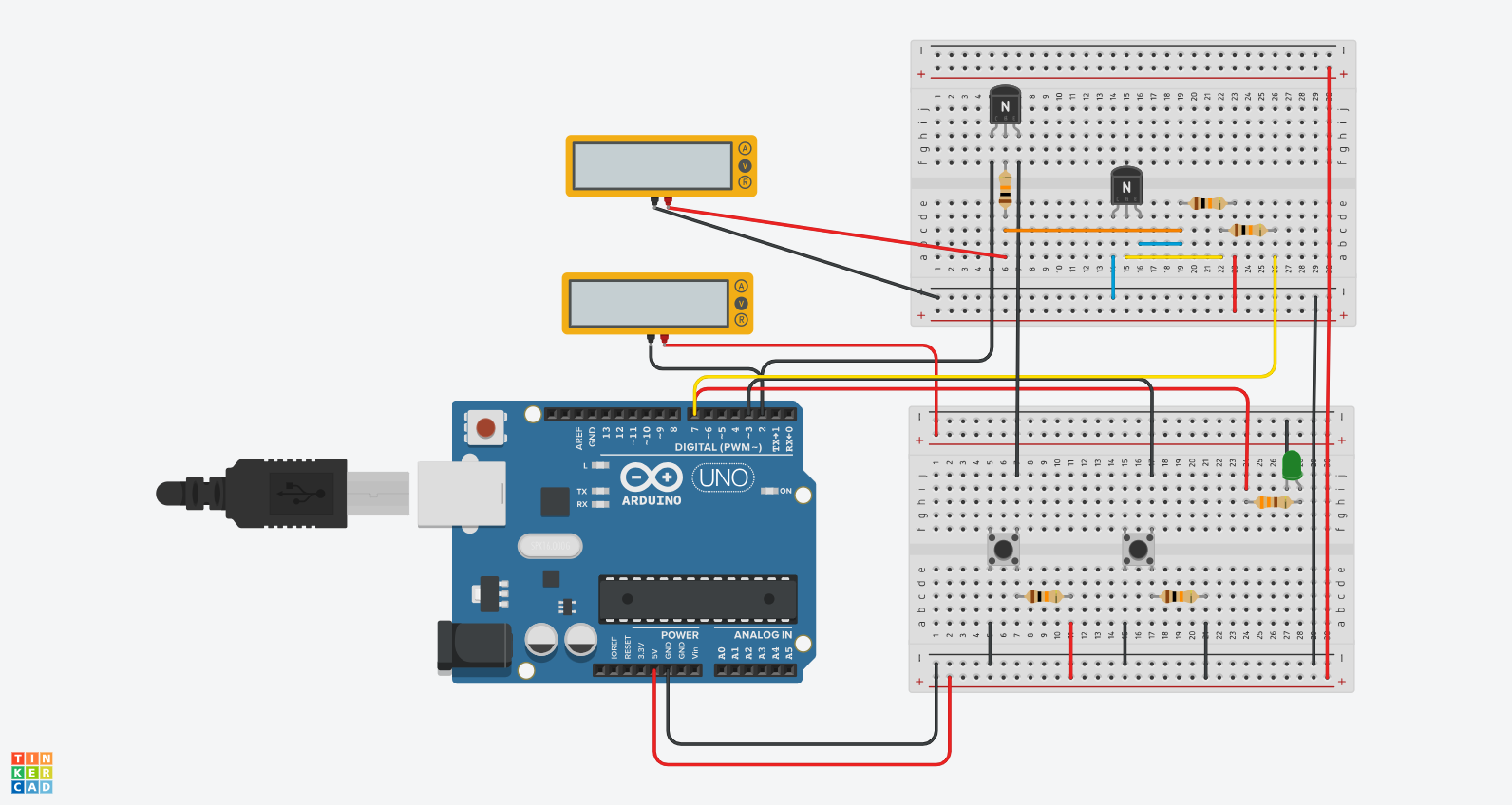
I built a circuit using an Arduino board that tests a logical inverter using NPN transistors. It works, but I'm trying to understand why it works.

circuit diagram of a logical inverter

The circuit consists of 2 push buttons:

  1. Left most button on bottom board. This is the Inverter test. When Pin7 is High, this button is disabled. When Pin7 is Low, pressing this button will bring Pin2 Low (causing the onboard LED to illuminate)
  2. Right most button on bottom board. This button brings Pin3 Low, which will toggle the state of Pin7.

The yellow wire is my input. When Pin7 is high, the green LED is lit and the input to the right most NPN transistor is high. This is where I am struggling to understand what is happening. When the base is brought high (via Pin7 being high), current flows from the blue line, through the transistor, and back to ground, correct? Why doesn't current also flow through the orange wire? I guess, there is a tiny bit of current that flows through (the virtual multimeter shows ~5mV).

I guess my understanding of electricity is that if a wire is connected to power like the orange wire is through the resistor, then it should have a charge, right? Why does the path through the transistor back to ground take priority when the base is high? Why aren't both paths (blue and orange) energized at the same time?

The final question I have is around power consumption. Will having these NPN transistors connected like this continuously draw current through the circuit? Should I be worried about the current draw if this circuit were battery powered?

If you'd like to explore the circuit, here is a link: https://www.tinkercad.com/things/925tzr3eQgD-logical-inverter?sharecode=HnrjlXw_c_-TWucWs_Mr8GE4MERS-WJjVebuuhAwDyk

EDIT

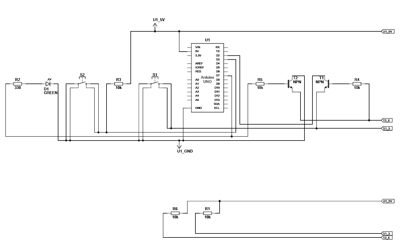
Here is the schematic. I need to get better at learning how to read these as well... I don't know what the bottom circuits are showing, or why they are not connected to main circuit.

Version B
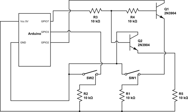
schematic

simulate this circuit – Schematic created using CircuitLab

Original somewhat en-visibilised schematic reloaded.
Both are a bit hard to read but together may be useful.

VERSION A

enter image description here

\$\endgroup\$
17
  • 1
    \$\begingroup\$ A proper schematic is needed. \$\endgroup\$
    – Andy aka
    Commented Mar 29 at 20:49
  • 3
    \$\begingroup\$ Can you draw a schematic? It saves everyone's time if you do it once, or everyone else that wants to answer your question must reverse-engineer your circuit implementation into a schematic. \$\endgroup\$
    – Justme
    Commented Mar 29 at 20:50
  • \$\begingroup\$ W.r.t. for the request for a schematic, upon following the link to the tinkercad circuit, clicking "Simulate" and then select "Schematic View" in the top right get a normal schematic view. \$\endgroup\$ Commented Mar 29 at 20:53
  • \$\begingroup\$ Just updated with a schematic. I also need to get better at reading them. \$\endgroup\$ Commented Mar 29 at 21:34
  • 4
    \$\begingroup\$ @joe_coolish While that is a schematic, it's simply all components put on a single line and a mess of wires routed between them. It is almost as difficult task to decipher what goes where than the original breadboard image. \$\endgroup\$
    – Justme
    Commented Mar 29 at 21:38

2 Answers 2

5
\$\begingroup\$

The schematic is very difficult to read.

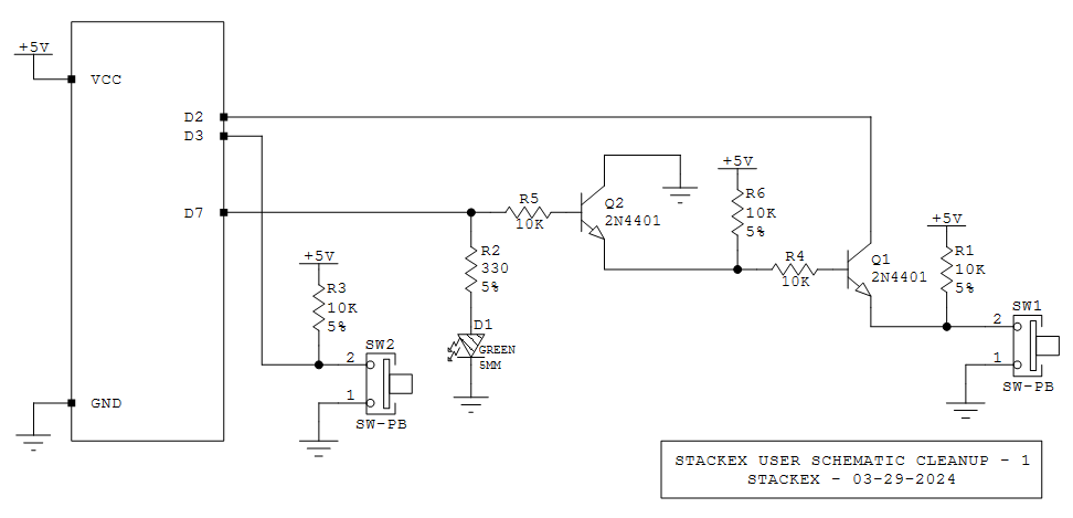
The T2 collector is tied to GND, so the it will not function as a normal transistor. It is not clear what your intent is for this signal.

In the text you refer to "Pin7", but there is no pin 7 on the schematic.

UPDATE:

Here is a first pass at a re-drawn schematic. I folded the two schematic sections into one. Based on this schematic, two of my previous comments have been deleted.

enter image description here

NOTE: When discussing the functions of individual components in a circuit, TinkerToy locations and wire colors are not good identifiers. Be clear about which schematic you are referring to, and use the reference designators on that schematic. For example, on my schematic the Q2 emitter is connected to the R4-R6 node.

UPDATE 2:

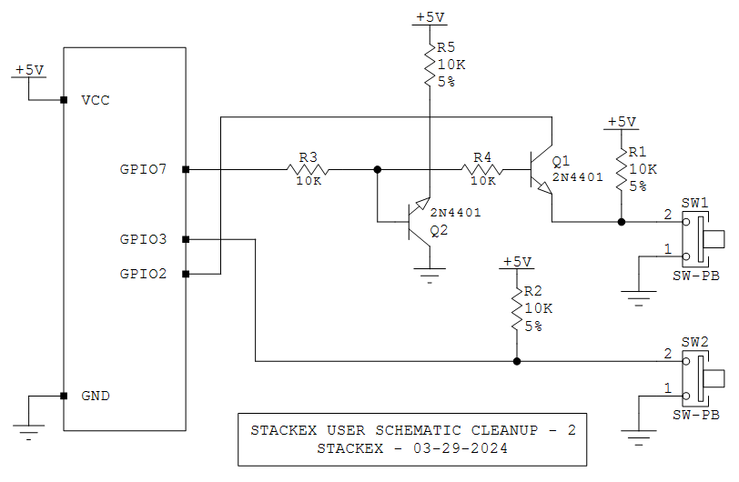
Here is a re-draw of the OP second schematic.

enter image description here

While there have been circuit changes around Q2, the connections around Q2 are very strange. Because the emitter is pulled up to Vcc, the transistor cannot conduct no matter what the base voltage is.

Also, it is not at all clear what the circuit is supposed to do.

\$\endgroup\$
4
  • \$\begingroup\$ Updated the OP with a schematic. \$\endgroup\$ Commented Mar 30 at 0:19
  • \$\begingroup\$ Q2 could be driven into reverse-active mode. Likely a mistake in the schematic, but it would still sort of work. Of course, with nothing actually connected to the output of this odd inverter, it's not exactly that useful. \$\endgroup\$
    – Hearth
    Commented Mar 30 at 4:56
  • \$\begingroup\$ The arrows in transistor symbols (and diodes, except Zeners) should point towards the more negative terminal of the power supply. (not necessarily be connected to the negative terminal, but headed that way). \$\endgroup\$ Commented Mar 30 at 6:13
  • \$\begingroup\$ The reverse breakdown base-emitter voltage usually is listed as 5 V or minimum for small-signal transistors. Depending on that would not be reliable in a 5 V circuit. This is almost certainly a schematic error. Still no word on the source of the circuit. \$\endgroup\$
    – AnalogKid
    Commented Mar 30 at 14:41
0
\$\begingroup\$

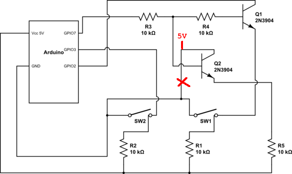
In your version B circuit, if no components are changed, the change below MUST be made for Q2 to conduct.

enter image description here

Both switches are either "strange" or worse in operation.

SW1 on means that Q1 when on is a hard short to ground of GPIO2.
That is not an approved way to treat an IO pin - but will often not cause damage.

SW2 when on shorts GPIO3 to ground.
This is even worse treatment of the IO pin.


With SW1 and SW2 open and the Q2 change shown above made:

GPIO2 low.

  • Q1 and Q2 always off

GPIO2 high.

  • GPIO7 high

    • Q1 on and R1 top goes high.
    • Q2 on and R5 top goes high
  • GPIO7 low

    • Q1 off and R1 top low.
    • Q2 off and R5 top low.
\$\endgroup\$

Your Answer

By clicking “Post Your Answer”, you agree to our terms of service and acknowledge you have read our privacy policy.

Not the answer you're looking for? Browse other questions tagged or ask your own question.