3
\$\begingroup\$

I was reading Computer Architecture and Organization 5th edition by Patterson and Hennessy. In Chapter 4, section 4.7 on Data Hazards, I read the following excerpt regarding forwarding from the MEM Stage:

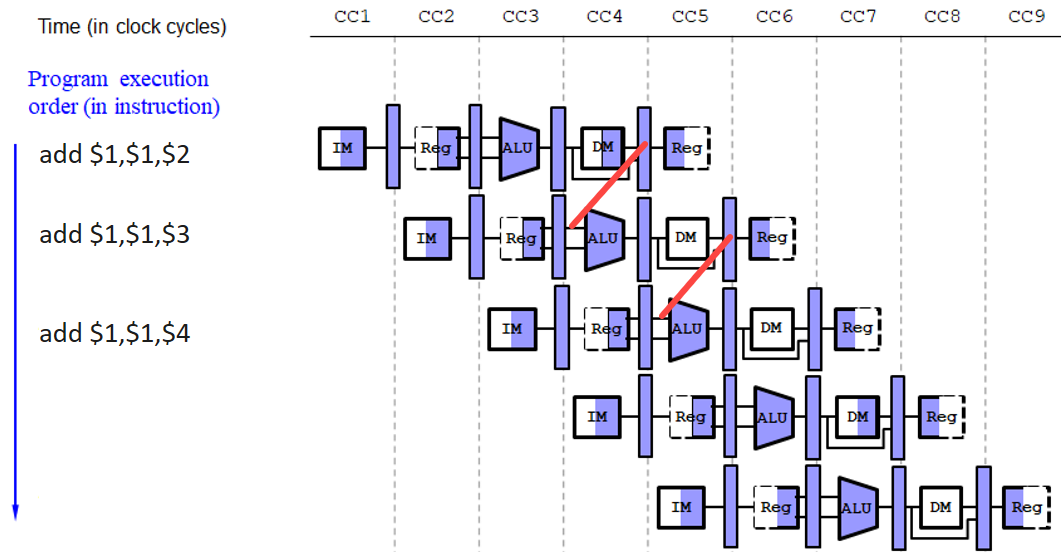
As mentioned above, there is no hazard in the WB stage, because we assume that the register file supplies the correct result if the instruction in the ID stage reads the same register written by the instruction in the WB stage. Such a register file performs another form of forwarding, but it occurs within the register file. One complication is potential data hazards between the result of the instruction in the WB stage, the result of the instruction in the MEM stage, and the source operand of the instruction in the ALU stage. For example, when summing a vector of numbers in a single register, a sequence of instructions will all read and write to the same register:

add $1,$1,$2
add $1,$1,$3
add $1,$1,$4

In this case, the result is forwarded from the MEM stage because the result in the MEM stage is the more recent result.

That confused me, bringing up the following questions:

  • When they say "forwarded from [x] Stage", does it mean from the [x]/... Pipeline Register or the .../[x] Pipeline Register? In this case, do they mean that the result is forwarded from the EX/MEM stage or the MEM/WB stage?

  • If it were to be from the MEM/EX stage, wouldn't that mean we would be going "backwards in time" as in the picture below? enter image description here

  • Since we are going "backwards in time", shouldn't the forwarding be like this below? enter image description here

  • This confusion may stem from the fact that I do not know which pipeline registers belong to which stage. That is, does every pipeline register that is between a stage belong to that stage or just the one from the right or the one from the left?

\$\endgroup\$

1 Answer 1

2
\$\begingroup\$

Let say, just for talking purposes, that $1=150, $2=300, $3=540, and $4=1000. (Decimal values.) And let's say that the addresses for these three instructions are at locations 0, 1, and 2. And that there are NOPs after that.

CC1    Present address 0 to the instruction memory. "ADD $1,$1,$2" presented to IF/ID.

CC2    Present address 1 to the instruction memory. "ADD $1,$1,$3" presented to IF/ID.
       Latch IF/ID, presenting $1 and $2 to REG file. REG outputs 150 and 300 to ID/EX.

CC3    Present address 2 to the instruction memory. "ADD $1,$1,$4" presented to IF/ID.
       Latch IF/ID, presenting $1 and $3 to REG file. REG outputs 150 and 540 to ID/EX.
       Latch ID/EX, capturing prior 150 and 300.
       Because there is no forwarding active, captured ID/EX values of 150 and 300 are
       presented to ALU.
       ALU summed output of 450 is presented to EX/MEM as an address and 2nd mux to
       ALU output of 300 is presented to EX/MEM as data.

CC4    Present address 3 to the instruction memory. "NOP" presented to IF/ID.
       Latch IF/ID, presenting $1 and $4 to REG file. REG outputs 150 and 1000 to ID/EX.
       Latch ID/EX, capturing prior 150 and 540.
       Latch EX/MEM, capturing address 450 and data 300.
       Because forwarding is active now, captured EX/MEM address value of 450 is
       selected by first input mux to the ALU while the captured ID/EX value of
       540 is selected by the second input mux. ALU summed output of 990 is presented
       to EX/MEM.
       $1 and 450 presented to MEM/WB by EX/MEM.

CC5    Present address 4 to the instruction memory. "NOP" presented to IF/ID.
       Latch IF/ID, presenting $0 and $0 to REG file. REG outputs 0 and 0 to ID/EX.
       Latch ID/EX, capturing prior 150 and 1000.
       Latch EX/MEM, capturing address 990 and data 540.
       Latch MEM/WB, capturing register $1 and address 450 (used as value.)
       Because forwarding is active now, captured EX/MEM value of 990 is selected by
       one of the input muxes to the ALU while the captured ID/EX value of 1000 is
       selected by the other input mux. ALU summed output of 1990 is presented to EX/MEM.
       REG file is presented prior register $1 and value 450 for writing.
       $1 and 990 presented to MEM/WB by EX/MEM.

CC6    Present address 5 to the instruction memory. "NOP" presented to IF/ID.
       Latch IF/ID, presenting $0 and $0 to REG file. REG outputs 0 and 0 to ID/EX.
       Latch ID/EX, capturing prior 0 and 0.
       Latch EX/MEM, capturing address 1990 and data 1000.
       Latch MEM/WB, capturing register $1 and address 990 (used as value.)
       Because there is no forwarding active, captured ID/EX values of 0 and 0 are
       presented to ALU.
       ALU summed output of 0 is presented to EX/MEM.
       REG file is presented prior register $1 and value 990 for writing.
       $1 and 1990 is presented to MEM/WB by EX/MEM.

CC7    Present address 6 to the instruction memory. "NOP" presented to IF/ID.
       Latch IF/ID, presenting $0 and $0 to REG file. REG outputs 0 and 0 to ID/EX.
       Latch ID/EX, capturing prior 0 and 0.
       Latch EX/MEM, capturing address 0 and data 0.
       Latch MEM/WB, capturing register $1 and address 1990 (used as value.)
       Because there is no forwarding active, captured ID/EX values of 0 and 0 are
       presented to ALU.
       ALU summed output of 0 is presented to EX/MEM.
       REG file is presented prior register $1 and value 1990 for writing.

At the beginning of CC8 the $1 register will have had its final value saved into it. (Presented at the end of CC7 and latched into the REG file somewhere around the start of CC8.)

Just read through the above and match up the details with your pictures. In CC4, where forwarding starts occurring, the EX/MEM value of 450 is pulled backwards via the forwarding units control signals to the input muxes that feed the ALU, so that the EX/MEM address value becomes one of the ALU inputs. That's why the red line shows as it does in your first diagram.

I think it is just a matter of you being able to read the intend of the person drawing that diagram. When you get stuck on something like this, just work through the steps like I did, above. It becomes a little clearer when you get out a piece of paper and just write out the details.
\$\endgroup\$
8
  • \$\begingroup\$ Took me a bit to digest the answer. It makes sense and I appreciate the detail. However, a couple of questions I have: The excerpt I read did not cover nops(yet). The nops added is due to the hazard detection unit? Also, by "that's why the red line shows as it does in your first diagram" Did you mean the second diagram? That is where I forwarded from EX/MEM as your explanation shows. \$\endgroup\$ Commented Apr 1 at 0:17
  • 1
    \$\begingroup\$ @JuanDeCastro There will also be other control information coming from ID/EX that can over-ride the forwarding unit's selections. So there are likely two muxes that follow the two muxes controlled by the forwarding unit. The forwarding unit makes its choices, but then the instruction operation itself makes different choices (like the PC, constant 0, constant 4 or whatever counts as a word size, or an operand.) Etc. I strongly recommend that you get out a stack of paper sheets. Use one for your register file. Use another for the ID/EX. And another for EX/MEM. And another for MEM/WB. \$\endgroup\$ Commented Apr 1 at 0:44
  • 1
    \$\begingroup\$ @JuanDeCastro Just run some assembly code and do it by hand. Just like you were playing dungeons and dragons and had to refer to a book of rules and the dungeon layout to play. Don't short yourself of the experience. Looking at pictures and reading a textbook is fine, I suppose. But there is nothing that comes close to just playing CPU by hand for a half hour or an hour. Deepens things into your soul. You will not forget, after. Not even 30 years later, you won't. It burns into you how things work. \$\endgroup\$ Commented Apr 1 at 0:49
  • 1
    \$\begingroup\$ Thank you for the detailed information and responses! I drew on paper the process of each stage and it definitely helped a lot. Thank you so much! \$\endgroup\$ Commented Apr 1 at 1:34
  • 1
    \$\begingroup\$ @JuanDeCastro No problem! I enjoy playing around with CPU designs as a hobby. I'm just glad you are also perhaps beginning to enjoy it! \$\endgroup\$ Commented Apr 1 at 1:40

Your Answer

By clicking “Post Your Answer”, you agree to our terms of service and acknowledge you have read our privacy policy.

Not the answer you're looking for? Browse other questions tagged or ask your own question.