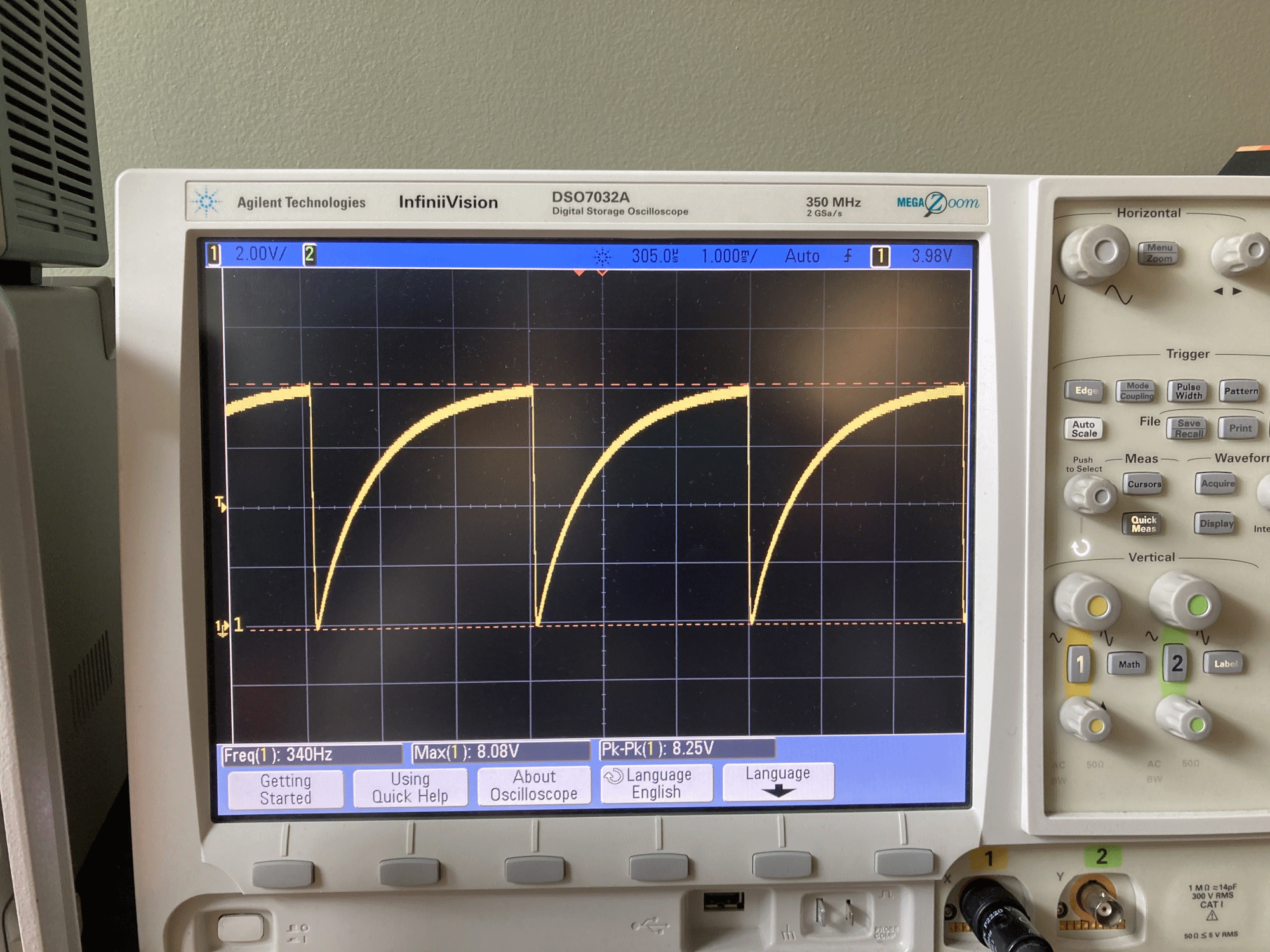
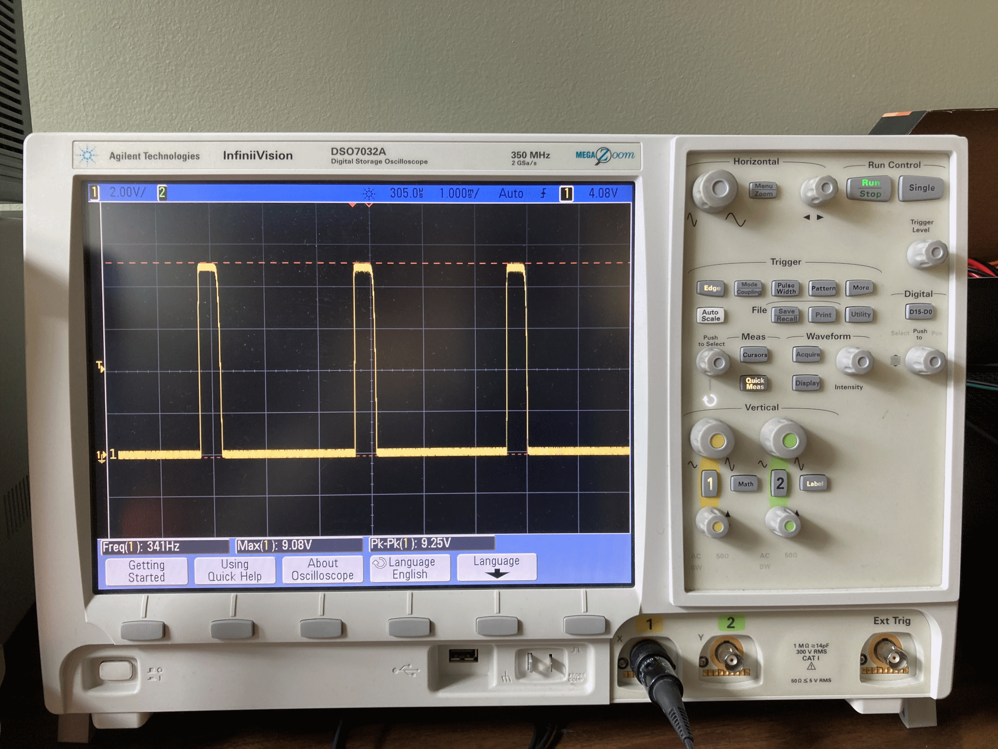
Firstly, fantastic job on your question! You've posted everything a reader needs: a schematic, parts list, photos, waveforms, and a good explanation of your problem - so have my up-vote!
OK, now to my answer:
Problem: The Protoboard does not match your Simulation
The main problem is that the logic gate used on the board does not match what was used in the simulation. The Schmitt-trigger inverter you used on the prototyping board is a CD40106B (I can see by the photo), whereas the one you used in your simulation is a 74HC14 (from your comment). Compared to the CD40106B, the 74HC14 is much faster, has different (lower) input voltage trip thresholds, has lower output resistance, and its power supply voltage is limited to 6V maximum. So your simulation will not match your scope waveforms because of this difference.
The other problem is parasitics.
Simulators can only be as good as the component model they have been programmed with. Many real-world components are not ideal; they have what are known as "parasitic elements" (abbreviated to just "parasitics"). By "parasitics" what I mean is electrical components that you cannot touch but which exist because of the way that real components are constructed.
For example, real-world diodes have what is called a "parasitic capacitance" connected across their terminals; this parasitic capacitance comes built-in to the diode, it is not a capacitor that you can touch and remove. Some simulators take this capacitance into account, some don't - and it depends on the diode model used for the simulation as to how closely the simulation results will match the real-world results.
Also, parasitics vary considerably between the different part numbers. For example, when it comes to diodes and their parasitic capacitance, a slow diode (like a 1N4004) has a much larger value for this capacitance than a fast diode (like a 1N4148). And that is not to say that all 1N4004 diodes have the exact same parasitic capacitance; there will always be some variation from instance to instance. So even if your simulation takes this parasitic capacitance into account, how accurately your simulation matches your real-world waveforms will depend on how closely the actual parasitics of the real-world component match the values of these parasitics used in the simulation model.
I hope you can start to see that parasitics have an important role to play in determining what is a good design and what is a bad design. A good design behaves in a predictable way regardless of the variation of parasitics that will occur with real-world components. A bad design may work just fine when you build one instance of it, but then stops working when you build another one using the same component part numbers because, for example, the parasitic capacitance of one of its diodes was different from the parasitic capacitance of the diode used in the first build.
How to Proceed From Here
As I see it, you have two choices.
Option 1. Tweak your simulation to get it to closely match the behaviour of your protoboard.
Option 2. Change your design to be more robust against component tolerances and parasitics, and hence much simpler to simulate.
Option 1.
This will take a long time. You will have to select the right simulator that is capable of doing the accuracy needed, learn how to use it, then ensure you have accurate models for each component. Then you would go through an iterative process: compare the results your simulation gives with the waveforms of the protoboard, note the differences, take a guess at which components are causing those differences, change the parameters (and parasitics) of the simulation, and repeat. Keep repeating until the simulation matches the scope waveforms to the accuracy required.
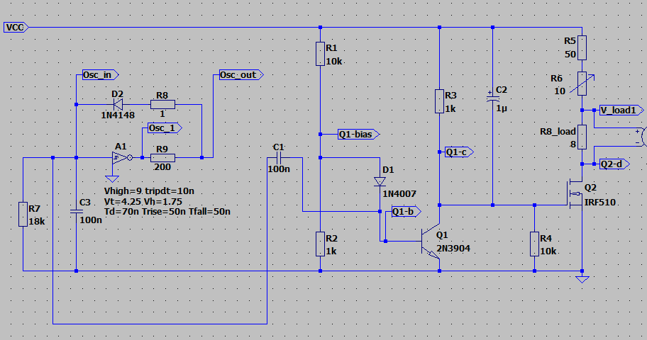
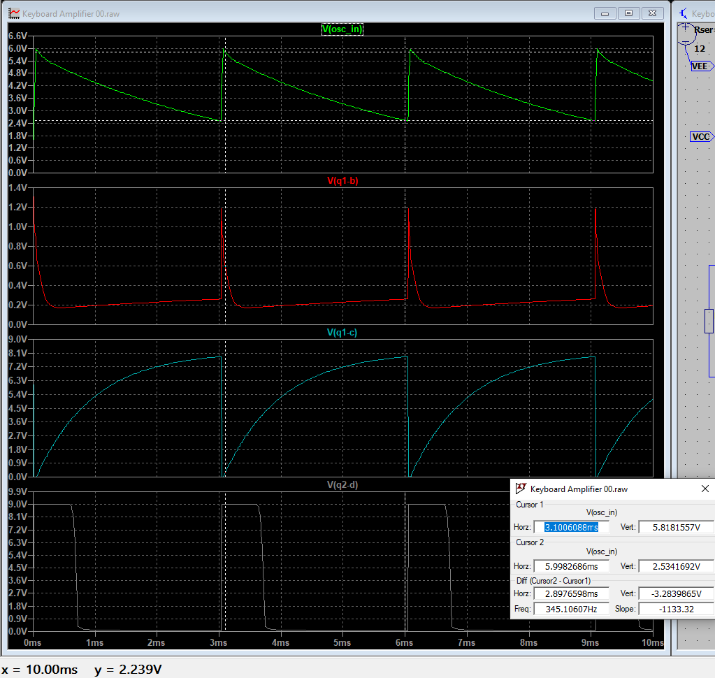
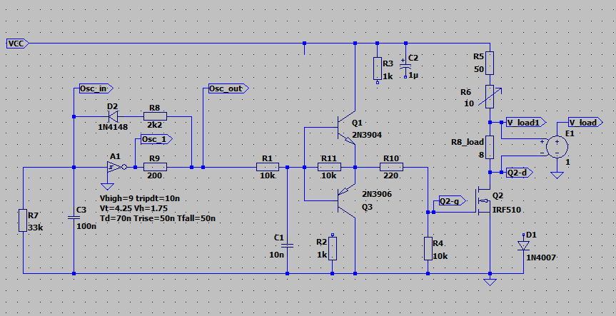
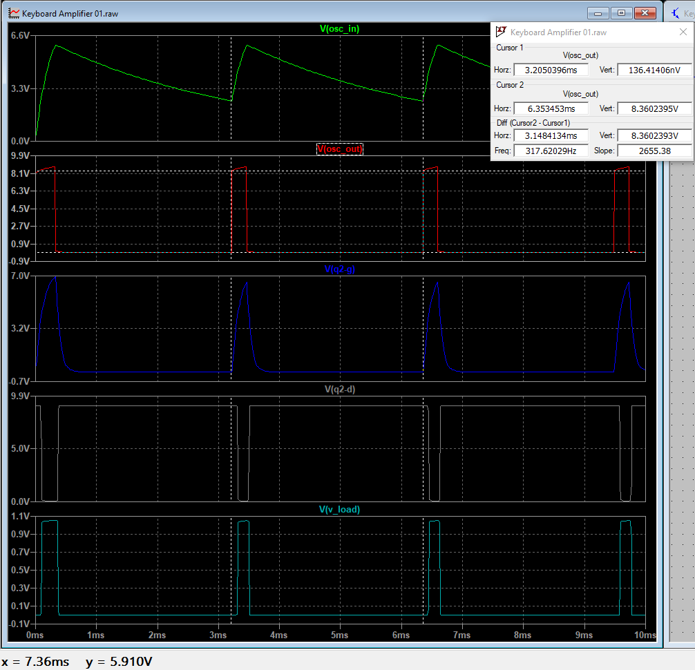
Using LTspice (refer images below), I managed to get waveforms that are similar, but not identical to those on your scope, however, my results depended upon me making adjustments to the following:
- Schmitt-trigger input voltage trip thresholds.
- Schmitt-trigger output resistance (R9 of my schematic, below).
- The parasitic capacitance of the diode connected to the base of the NPN (D1 of the schematic below).


.
Option 2.
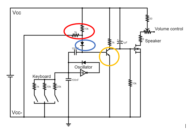
As it now stands, your circuit design is not tolerant of parasitics and component variations. The main example of this problem is how the NPN is connected to the oscillator. Usually, the stage following a logic gate is connected to the output pin of the gate. However, in your circuit, the NPN base is coupled (via a capacitor) to the input pin of the logic gate, not the output pin.
So even if you were to get the Schmitt-Trigger of your sim to have the same trip voltages as the one on your protoboard, you would then need to precisely model how much the next stage loads the node at the Schmitt-Trigger input pin.
To get a more predictable design that is far more tolerant of parasitics and component variations, you should connect the base of the NPN to the output pin of the logic gate - however, this needs to be done with some caution.
Simply connecting the 100n capacitor (C1) to the output pin of the Schmitt-Trigger could damage the NPN transistor due to excessive reverse voltage applied to its base. This is because the base will now be receiving a much stronger pulse: 9V peak with fast edges. This could cause strong reverse voltage on the base of the NPN, which may damage it. If you tried this, the actual results you get on the protoboard will be very dependent on the type of diode connected to the base of that transistor, and the parasitics of various components and wiring.
So let's review your design, and look at some suggested changes.
Review of Your Schematic
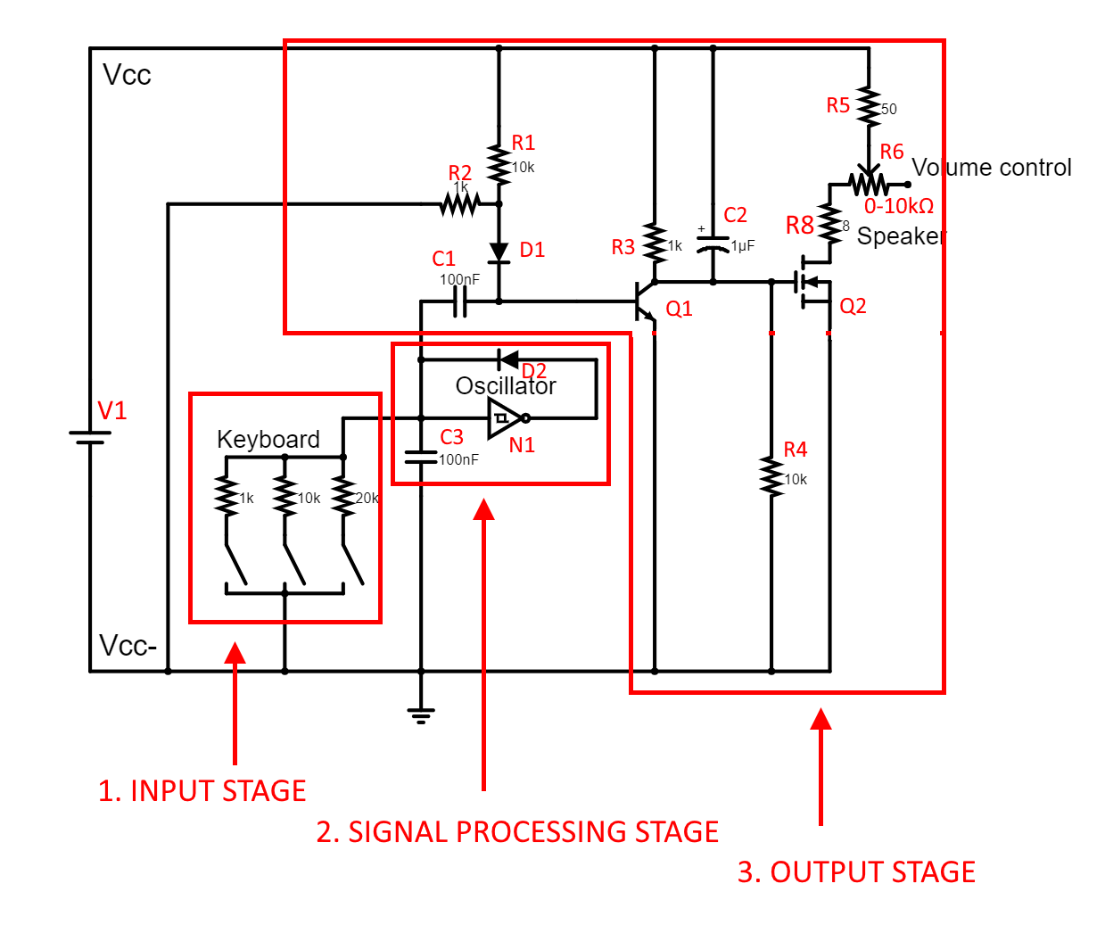
I can see that your circuit is made up of three main sections:
- An input stage (the "keyboard").
- A signal processing stage (the oscillator).
- An output stage (the amplifier that provides electrical power to the output device, in this case, a speaker).
I have marked-up your schematic and added component identifiers, refer image below:

Image above: Original schematic from question (with red-ink mark-ups by answerer).
Suggested Changes to the Design
The suggested changes are captured in the schematic below. I have preserved the component IDs from the previous schematic as much as possible. Several of the components on your current design are now unused, these are shown on the schematic as the components connected by only one pin. Changes are listed below the schematic.

Main changes:
- Output of the oscillator moved to the output pin of Schmitt-trigger.
- Added R8 to limit the current supplied by the output pin of Schmitt-trigger into timing capacitor C3 during the brief re-charge time.
- Gate drive current for MOSFET Q2 is provided via a buffer stage, formed by using the previous NPN (Q1) and a new PNP (Q3), both configured as emitter-followers.
Due to these changes, the circuit behaviour is now far more tolerant of parasitics, and hence your simulation results should be a much closer match to the protoboard. The key parameters to get right are the trip voltage thresholds for the Schmitt-trigger; once these are set correctly, the simulation should match the scope waveforms quite well.
Waveforms:

Other Improvements:
Less power is drawn from the power supply. The voltage buffer
formed by Q1 & Q3 only draws significant current when the gate
voltage on the MOSFET Q2 is changing. The static current is almost
zero when Q2 gate is OFF, and only ~1mA when Q2 gate is ON (due to
current in R4).
Output of Schmitt-trigger chip is no longer heavily loaded during C3 re-charge time, R8 ensures the output current from the Schmitt-Trigger is within device limits, and not dependent upon parasitics (output resistance of chip, and resistance of diode D2).
Oscillator frequency and waveform is far less dependent on the loading effect of the following stage.
Other features:
- Adjust the ON time of the MOSFET Q2 by adjusting R8.
- Adjust the "tone" of the sound by adjusting R1 & C1.
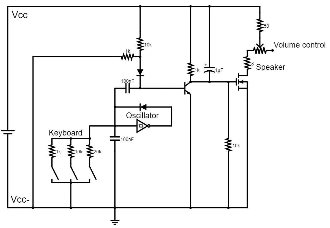 Note: the 1k resistor that is connected to the collector of the first transistor is actually 100 ohm.
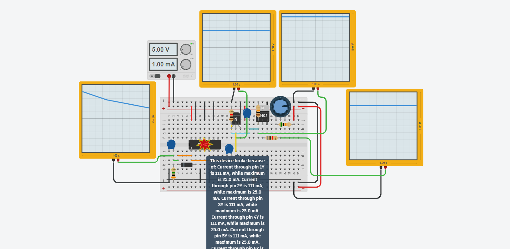
 The wires that are not connected to anything are:
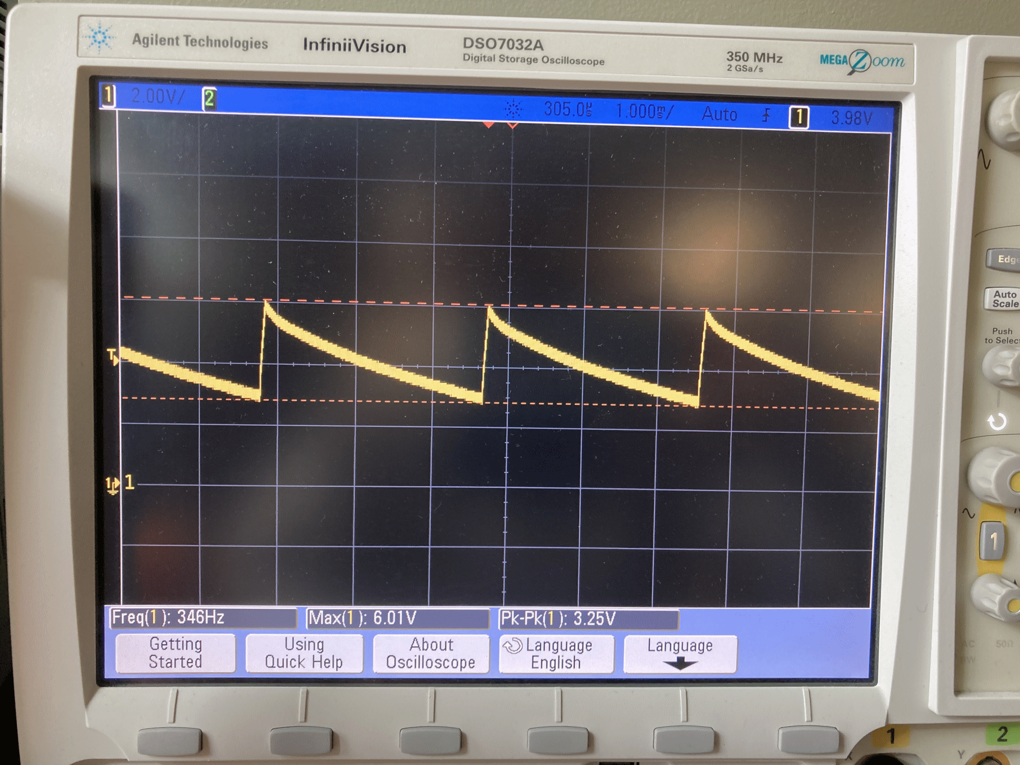 Oscillator out (connected to the input pin of the inverting schmitt trigger)
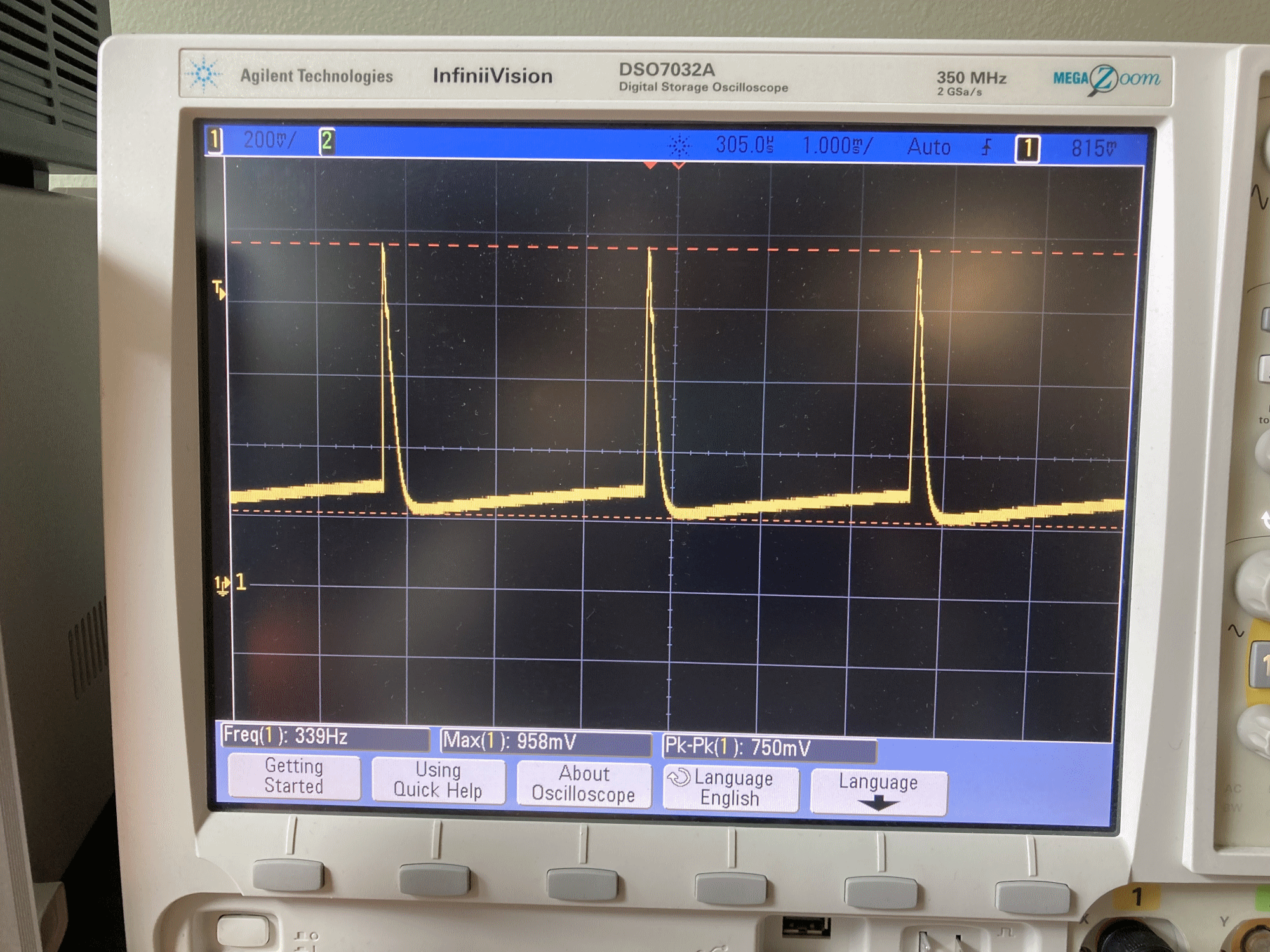 transistor base (current and voltage that flows into transistor base)
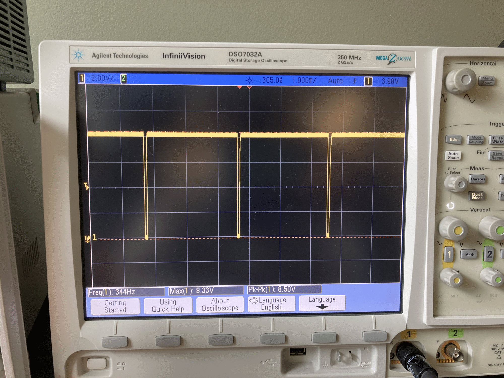 transistor out (collector) (this one is taken in the same place as the next oscilloscope screen but without the polarized capacitor.
