3
\$\begingroup\$

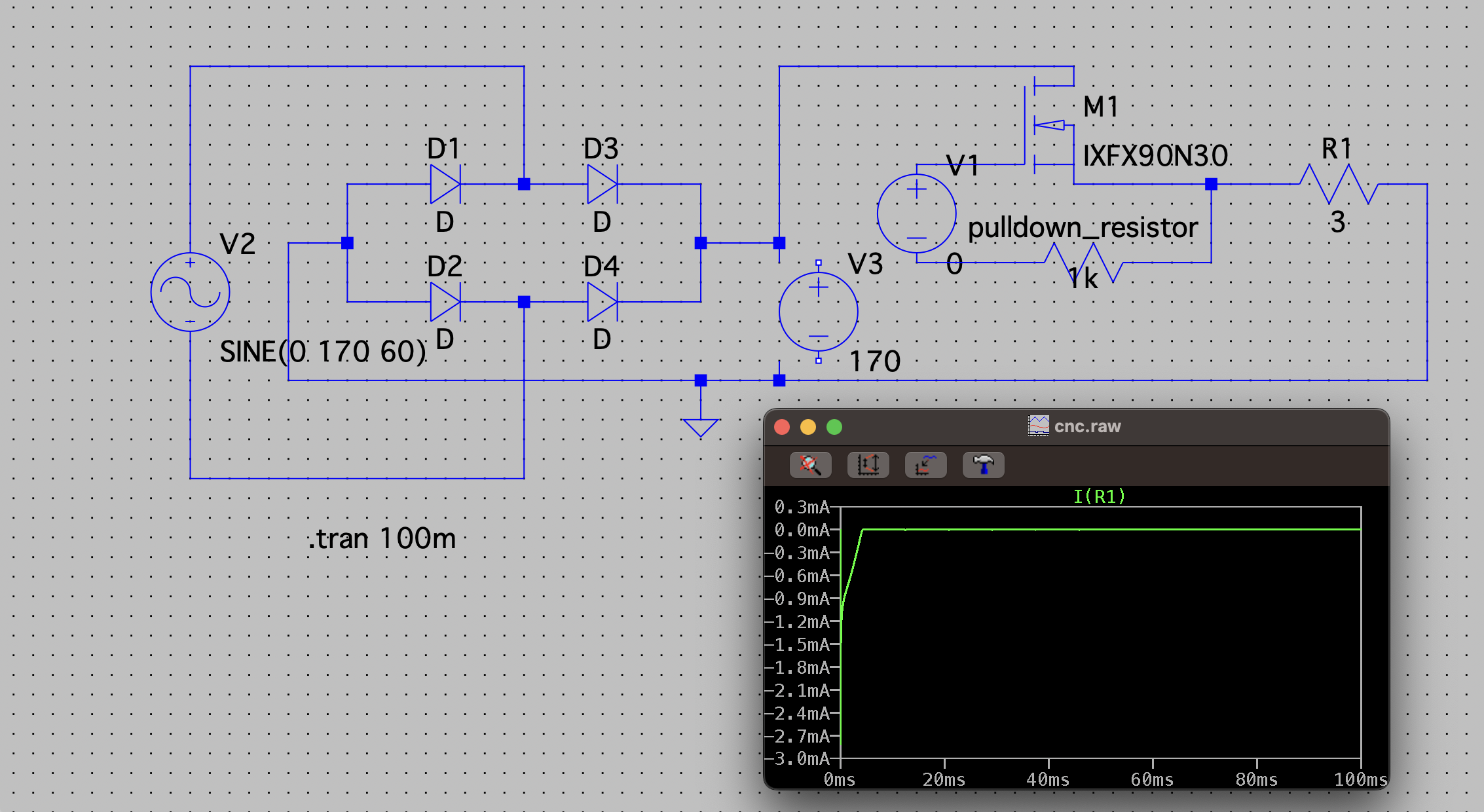
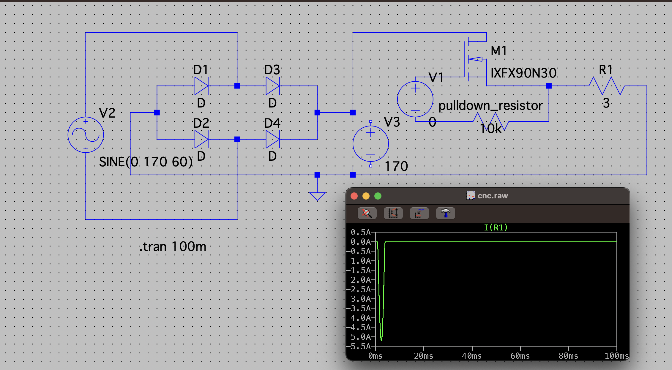
I've been having some trouble getting a pulldown resistor to behave as expected in LTspice. Here are two screenshots of my circuit.

enter image description here

enter image description here

This circuit has a full wave bridge rectifier convert AC (USA household wall voltage) into DC, which then goes into a power MOSFET to drive a load (motor). The only difference is the change in pulldown resistor value from 10k -> 1k, and as you can see the 10k resistor makes the load draw a transient 5 amps (the negative is just cause of the direction). This doesn't make any sense because \$V_{GS}=0\$ in both cases so the MOSFET should be off. I tried replacing the rectifier with a pure DC voltage source (V3 in screenshot), and the transient current effectively disappears. I am wondering if this is some numerical simulation failure in LTspice or if this is truly indicative of real-world MOSFET behavior, e.g. hand-wavily perhaps some AC component of the rectified DC signal and the parasitic capacitance in the MOSFET can cause the pulldown resistor value to matter.

Anybody have ideas? Relatively new user to LTspice here, so open to all advice/suggestions.

PS: the sim window says 'cnc.raw' because this is a simulation of the metal CNC that I've been fixing :)

\$\endgroup\$
6
  • \$\begingroup\$ Is V1 representative of some kid of logic device (e.g. microcontroller)? If so, and you want to use an N-channel MOSFET you should swap the position of it with the 3ohm resistor. Otherwise, look into using a P-channel MOSFET. Referencing your gate to the load is going to cause this spike problem for you when the MOSFET is supposed to be OFF, but also give you trouble when you try to turn the MOSFET ON. \$\endgroup\$
    – Ste Kulov
    Commented May 20 at 21:13
  • \$\begingroup\$ One more comment. You believe that \$V_{GS}=0\$, but you should actually plot it and see. You can do that by clicking on the gate node, and then holding the click and releasing it when the mouse cursor is on the source node. \$\endgroup\$
    – Ste Kulov
    Commented May 20 at 21:23
  • \$\begingroup\$ @SteKulov Yeah, V1 represents an Arduino PWM on the gate to get variable motor voltage and hence spindle speed. Do you have a resource explaining why N-channel MOSFETs should only be used as a low-side switch? I naively figured it didn't matter from the main circuit's perspective because the switch either makes the circuit open or closed. I also naively figured the microcontroller circuit could be referenced anywhere, as long as KVL/KCL analysis makes sure no excessive voltage/current goes into the microcontroller circuit. \$\endgroup\$
    – but_why
    Commented May 20 at 21:40
  • \$\begingroup\$ @SteKulov Interesting, the \$V_{GS}\$ spikes to 4.0, so you are right. \$\endgroup\$
    – but_why
    Commented May 20 at 21:45
  • \$\begingroup\$ I don't know of any resource off the top of my head. I can try to give the gist of it. It's easier to control a MOSFET when the source is at a fixed potential, that way you can easily control the gate voltage required for turn ON or OFF. In low-side switch configuration the N-channel source will be at GND, and always at GND. If you try to do what you're doing, then source voltage will not be fixed and will change whether it's ON, OFF, or between ON & OFF. You can get around this with a special gate driver IC which boosts the voltage of the gate by tracking what's at the source. \$\endgroup\$
    – Ste Kulov
    Commented May 20 at 21:52

3 Answers 3

4
\$\begingroup\$

There are a few problems with the circuit, the first is you have a disconnected supply, which will create problems for the solver matrix. Delete V3 if you aren't using it. The second problem is the dc solver that starts at the beginning of the simulation and decides what the initial conditions are. This is getting confused because V1 is essentially floating. It would be good to attach a 1GΩ resistor to ground to help the solver find the DC initial conditions.

The last thing is it could be a not so great mosfet model. A lot of times the models are 'fudged' with active components such as voltage sources in the subcircuit model that can do weird things when connected to non-standard circuits, a Nfet should be used in a low side switch.

Edit:

Actually, you should put the 1k to ground and put it on the gate, reference V1 to ground also. Another thing to try is put in 0.1Ω of resistance in series with the gate to simulate real copper.

\$\endgroup\$
5
  • 1
    \$\begingroup\$ Seems like a standard built-in VDMOS model, so I don't think the 2nd part applies. But I agree the N-channel shouldn't be used like this (high side switch) without a boosting gate driver. \$\endgroup\$
    – Ste Kulov
    Commented May 20 at 21:16
  • \$\begingroup\$ I tried moving the switch to the low side and deleting V3, both didn't change much. When you say "It would be good to attach a 1GΩ resistor to ground to help the solver find the DC initial conditions", where is this resistor attached? Is it from the - terminal of V1 to ground (in low side switch configuration)? Cause that didn't change anything. \$\endgroup\$
    – but_why
    Commented May 20 at 21:59
  • 1
    \$\begingroup\$ Actually, you should put the 1k to ground and put it on the gate, reference V1 to ground also. Another thing to try is put in 0.1Ω of resistance in series with the gate to simulate real copper. \$\endgroup\$
    – Voltage Spike
    Commented May 20 at 22:01
  • \$\begingroup\$ @but_why It's probably because your model of how the Arduino connects to the system is incorrect. It should look more like this (although this is over-simplified too): i.sstatic.net/OxibIP18.png . You might also want to look into a "freewheeling diode" or "flyback diode" to protect the MOSFET when driving an inductive load such as a motor. Also keep in mind of Fabio's answer, which can apply when the Arduino is not powered on and looks more like a high-impedance instead of a voltage source. A lower-valued pulldown resistor can help with this scenario. \$\endgroup\$
    – Ste Kulov
    Commented May 20 at 22:18
  • 1
    \$\begingroup\$ Ah, yes putting V1 and the pulldown resistor in parallel makes it work! That makes more sense. And yes, in the real circuit diagram I have a diode that connects to the positive voltage line. \$\endgroup\$
    – but_why
    Commented May 20 at 22:27
2
\$\begingroup\$

The unexpected current in the MOSFET is due to the Miller effect. The parasitic capacitor between drain & gate is passing sufficient charge to the gate to partially turn on the MOSFET. There is a minimum value of resistance required at the gate of the MOSFET to keep the voltage due to this drain-to-gate current from reaching the gate-source threshold voltage. You can confirm this by using the simulator to observe Vgs.

\$\endgroup\$
3
  • \$\begingroup\$ Is there a reason this effect would only be transient rather than steady-state? Or do you have a good resource for me to learn about this behavior in a MOSFET? \$\endgroup\$
    – but_why
    Commented May 20 at 22:16
  • \$\begingroup\$ @but_why You can try this but it doesn't cover your use-case. Assuming the Arduino is not there, there is an RC circuit formed by the MOSFET parasitic Cgd and the pulldown resistor. You can get a rough estimate of these parasitic capacitors by running a .op simulation and pulling up the error log (CTRL+L). Then you can simulate the equivalent circuit and see where the currents are flowing. \$\endgroup\$
    – Ste Kulov
    Commented May 21 at 9:18
  • \$\begingroup\$ @but_why Here you can see that the current through Cgd (due to charging the drain node to the steady state voltage) goes through the 10K resistor and induces a large voltage there. You can reduce this by decreasing the pulldown resistor value, which is effectively what your Arduino GPIO will do when driving a HIGH or LOW. Keep in mind that the values resulting from the equivalent circuit aren't accurate, but it at least lets you see the capacitive behavior split up between all three terminals. \$\endgroup\$
    – Ste Kulov
    Commented May 21 at 9:24
1
\$\begingroup\$

To get your pull-down to behave as you want, you really need your N-type MOSFET to be a low side switch. In your configuration, the gate can effectively float and lead to undesirable behavior.

As mentioned in a comment on your original question, high side switching of an N-type MOSFET is doable but requires extra circuitry to boost your control signal above the voltage at the source terminal. Typically, your controller doesn't have that available and you need to add some form of boost circuitry (there are plenty of single IC options to do this) to achieve that. -- another point to something in that comment thread: you're correct in saying that the microcontroller doesn't care about its reference, but you're going to have a devil of a time with the Arduino and communicating with it if it's floating like that. Make it easy on yourself and don't float the board, else risk a lot of other strange behaviors

\$\endgroup\$

Your Answer

By clicking “Post Your Answer”, you agree to our terms of service and acknowledge you have read our privacy policy.

Not the answer you're looking for? Browse other questions tagged or ask your own question.