2
\$\begingroup\$

I am playing around with charge pumps / voltage doublers for the first time and have some questions that I can't find anything online to.

First, I have a standard charge pump, in an ideal world the voltage is doubled on the output, when given a 50% duty cycle PWM but what happens if I change that duty cycle to more or less than 50% ? I expect that I would be able to "tune" the output from Vcc to 2*Vcc or am I missing some real world practicalities here ? I do not get my expected output when I adjust the duty cycle, so I started looking around for an answer. The equations I have found don't take into account the duty cycle ( from what I have found ) is it just a standard fact that with voltage doublers the PWM DC is always 50% ?

Second question is if I have a 12Vcc into the charge pump, but I use a 5V PWM signal, will I get 17V ( ideal world again ) output ? I have not played with this yet as I really do not want to break my MCU, I don't immediately see something breaking but I wanted to ask before I head down that possibly risky road. ( I only have one MCU right now to play with )

From things I have found online I think I have a general understanding of them, but only in the "original design specs" I feel like adjusting things should give me what I want / expect to see but I don't have any background to draw on here yet.

\$\endgroup\$
1
  • \$\begingroup\$ I'd recommend reading this EESE post closely. It may cover some part of what you want. \$\endgroup\$ Commented Jun 4 at 6:49

2 Answers 2

2
\$\begingroup\$

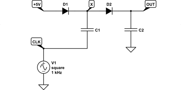
Changing the frequency or duty cycle won't change the ultimate long-term charge (voltage) across the output capacitor of the charge pump. I'll explain why here. I don't know what exact design you are using, but it will be some variation on this:
schematic

simulate this circuit – Schematic created using CircuitLab

The diodes behave like switches, opening and closing as the potential difference across them changes polarity. In practice they are not ideal, having some non-zero voltage across them (0.7V) when "closed", but to understand this circuit's behaviour, they can be envisaged as switches, either open or closed. Some designs (such as the implementation inside the famous ICL7660) employ transistors to exhibit more "ideal" behaviour (more closely mimicking actual switches), but the principle of operation remains the same.

During times when the CLK node is low (0V), D1 becomes forward biased, and conducts. This quickly charges C1 up to 5V:

schematic

simulate this circuit

When CLK rises to +5V, the lower terminal of C1 rises with it, taking node X above +5V in potential. D1 becomes reverse biased, no longer conducting, and D2 becomes forward biased, like a closed switch. This, then is the equivalent situation:

schematic

simulate this circuit

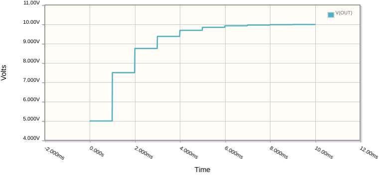
In this condition, with the potential of node X now above OUT, current \$I\$ flows, charging C2 beyond 5V also. OUT doesn't immediately rise to +10V, since current stops flowing when the two capacitors have the same charge (assuming C1 = C2). However, this process repeats, and C2 is charged a little during every cycle. Eventually C2's voltage approaches close enough to 10V to call it 10V. The result is a stepped rise of \$V_{OUT}\$, which is clear in a simulation:
enter image description here

To understand why changing the frequency or duty cycle of the CLK source has no (or little) effect on the long-term voltage across C2, it is necessary to see that the voltages across C1 and C2 change extremely rapidly. This is clearly visible in that graph; the vertical edges are just that - vertical, indicating that the charging and discharging of those two capacitors is instantaneous.

In real life those voltage transitions will not be instantaneous, of course, because the +5V source, and the CLK signal itself have some impedance which will slow the rise and fall of voltages across the capacitors, but the point here is that those transitions are very rapid. Once the system has settled following each CLK edge, nothing else happens. There are no changes occurring between those edges, everything happens immediately following the transitions of CLK.

These charging/discharging/transfer operations happen in microseconds, with nothing else going on for long durations (perhaps milliseconds) in between those transitions. Changing the frequency or duty cycle of CLK will only alter the duration between transitions, and will not significantly affect the amount of charge gained or transferred by the capacitors at each transition.

Ultimately, unless you can control how much charge is gained/transferred at each CLK transition, you have no control over the ultimate charge of C2, which means that PWM cannot help.


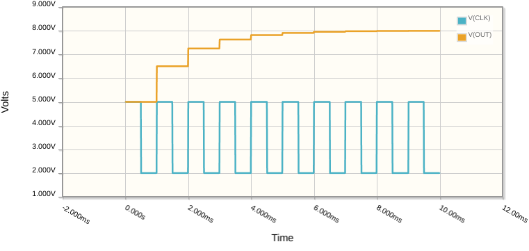
If you wish, you can produce a voltage lower than 10V at OUT by reducing the voltage that C1 charges to. For example, if you can somehow make CLK oscillate between +2V and +5V, then the difference (3V) will be added to C2's initial charge (+5V), for an eventual output of +8V:
enter image description here

\$\endgroup\$
4
  • \$\begingroup\$ Thank you for the detailed explanation, I don't mean to push my luck here, but could you explain why the PWM signal would need to be between 2 and 5V in that example ? Why would a 0-3V PWM with a 5V input not also work to give 8V ? I feel as if I'm missing something important around this part of it all. \$\endgroup\$
    – Spider999
    Commented Jun 4 at 11:46
  • \$\begingroup\$ @Spider999 OK, to obtain 8V, which is 3V above the supply, C1 must charge to have a potential difference of 3V. Since during the C1 charging phase \$V_X=+5V\$, then you require CLK to be 3V lower than that, \$V_{CLK}=+2V\$. Then when CLK rises to +5V, X rises with it, but 3V higher, to +8V. \$\endgroup\$ Commented Jun 4 at 11:56
  • \$\begingroup\$ @Spider999 That said, I think that CLK could go between 0V and +3V and have the same effect. Your question is a good one, but I haven't simulated that. Essentially, whatever peak-to-peak amplitude of oscillation at CLK will be added to +5V. \$\endgroup\$ Commented Jun 4 at 12:01
  • \$\begingroup\$ Yea the way I'm understanding it it's just pushing up (adding) whatever the voltage "swing" is on the PWM signal when high to the supply. Thanks, ok so it shouldn't break anything, I'll test it out and report back. \$\endgroup\$
    – Spider999
    Commented Jun 4 at 21:38
2
\$\begingroup\$

what happens if I change that duty cycle to more or less than 50% ?

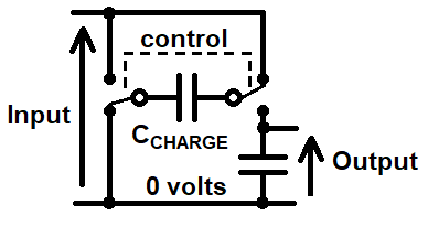
Duty cycle manipulation does not adjust the output voltage in a simple charge pump. Consider this simplified circuit that uses switches operated at high frequency: -

enter image description here

With the control input setting the switches as shown, \$C_{CHARGE}\$ is connected to the input voltage. Then, when the control input reverses the switches, the charged \$C_{CHARGE}\$ is placed in series with the input supply and simultaneously connected with the output capacitor: -

enter image description here

After several cycles of switching back and forth, the output capacitor is charged to twice the input voltage.

This means that altering the duty cycle of the control input can only ever control the speed at which the output capacitor becomes charged.

Second question is if I have a 12Vcc into the charge pump, but I use a 5V PWM signal, will I get 17V ( ideal world again ) output ?

The simple and straightforward answer is no. The control signal (5 volts) is for operating the switches and, it's level has nothing to do with the charging process. Clearly, the that level is too low, the switches (think of them as electromagnetic relays if you wish) will fail to operate.

\$\endgroup\$

Your Answer

By clicking “Post Your Answer”, you agree to our terms of service and acknowledge you have read our privacy policy.

Not the answer you're looking for? Browse other questions tagged or ask your own question.