4
\$\begingroup\$

Help me to understand how this oscillator works. Although I mostly want the vintage computer to work, I also want to understand how this circuit functions.

I attempted to recreate the oscillator on a breadboard, but did not get it to oscillate. I verified the crystal works by connecting it to a signal generator with a 50 ohm resistor in series. At 9.808 MHz, the Vp-p increases dramatically. I also verified the capacitors (up to 1 KHz). My equipment and supplies are reasonable for a hobby lab (o-scope. sig-gen, LCR meter, good supply of components).

Some questions:

  1. How can I test the transistor?
  2. Am I testing the crystal properly?
  3. How does this oscillator oscillate?

Background

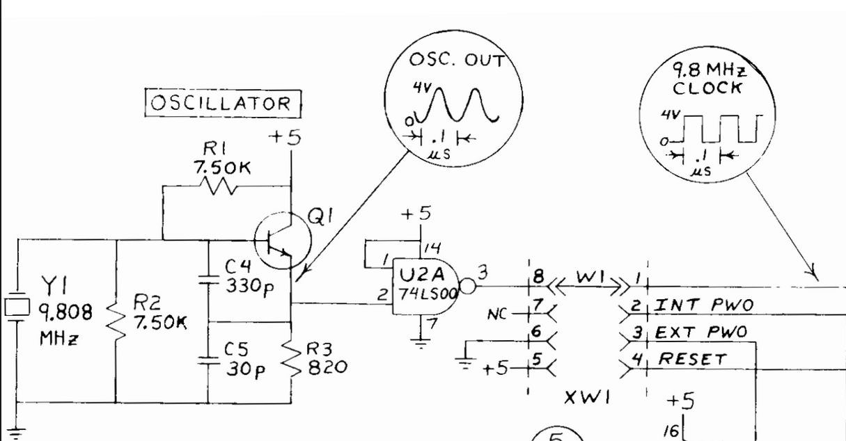
This is the oscillator from a 1980's vintage Hewlett Packard computer. Mine has a bad transistor Q1. Cold spray on Q1 allowed the computer to operate normally. Next, I removed jumper W1 and injected a 9.808 MHz square wave into XW1-1, and the computer operated normally for 24h. I also measured at U2-2 (the oscillator output / input to NAND). The peak was around 2.4 V, and the frequency was correct at 9.8 MHz.

Good people at the HPSeries80 group identified the transistor as a 2N3563 with these properties

Type# Dec LeadID Vcbo Min Vceo Min Vebo Icbo Vcb Hfe @Vce @Ic Cob-Max fT-Min
PN3563 NPN RF OSC EBC 30v 12v 2.0v 50nA 15v 20 to 200 10 8.0mA 1.7 600Mhz

I didn't ask for the crystal oscillator properties.

The oscillator

From the HP85A schematic

enter image description here

My best recreation (disregard crystal parameters):
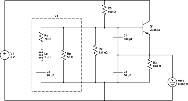
schematic

simulate this circuit – Schematic created using CircuitLab

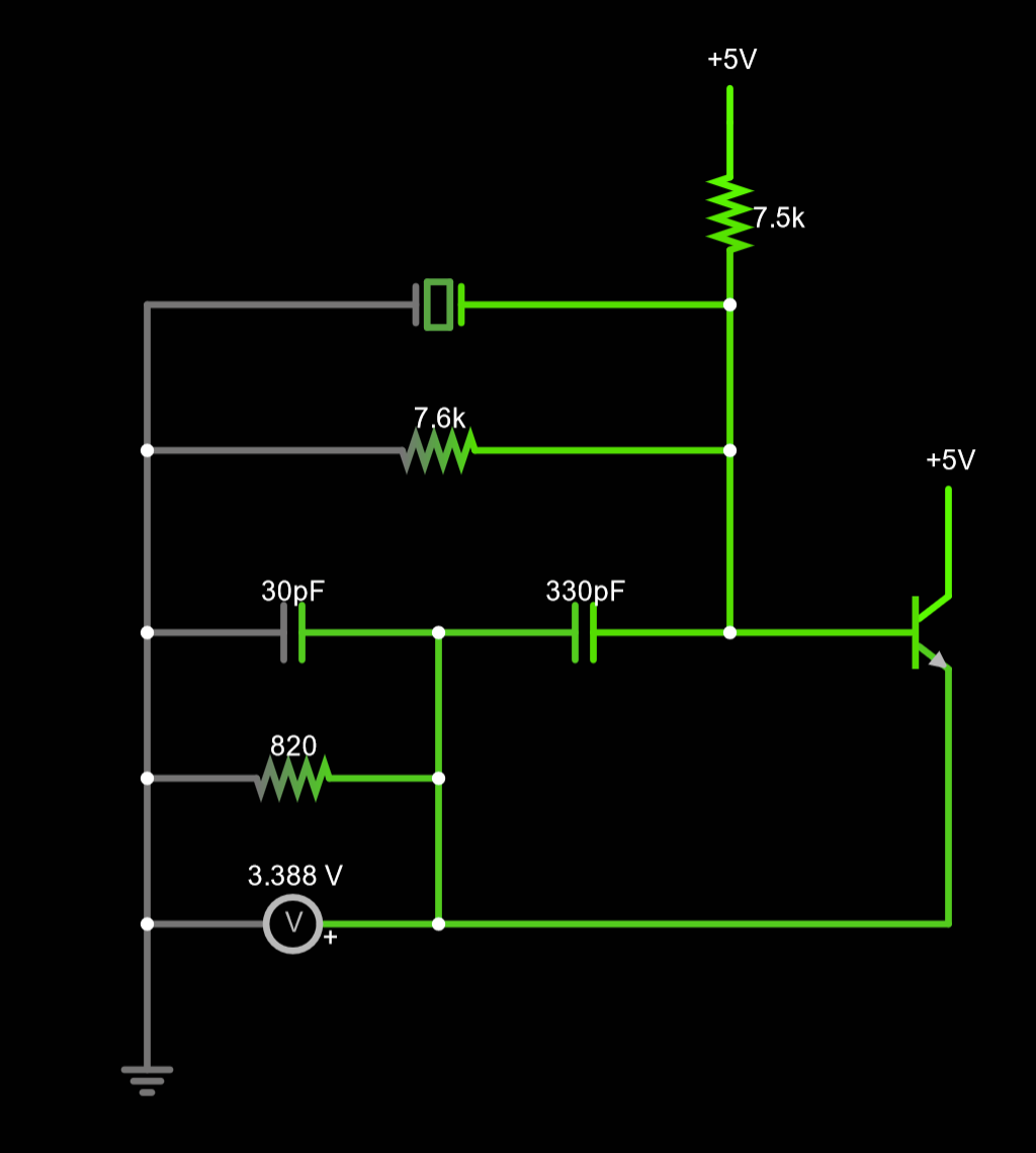
and in Falstad Falstad circuit diagram of a 9.808 MHz oscillator
\$\endgroup\$
1

4 Answers 4

5
\$\begingroup\$

Explain how this crystal oscillator works

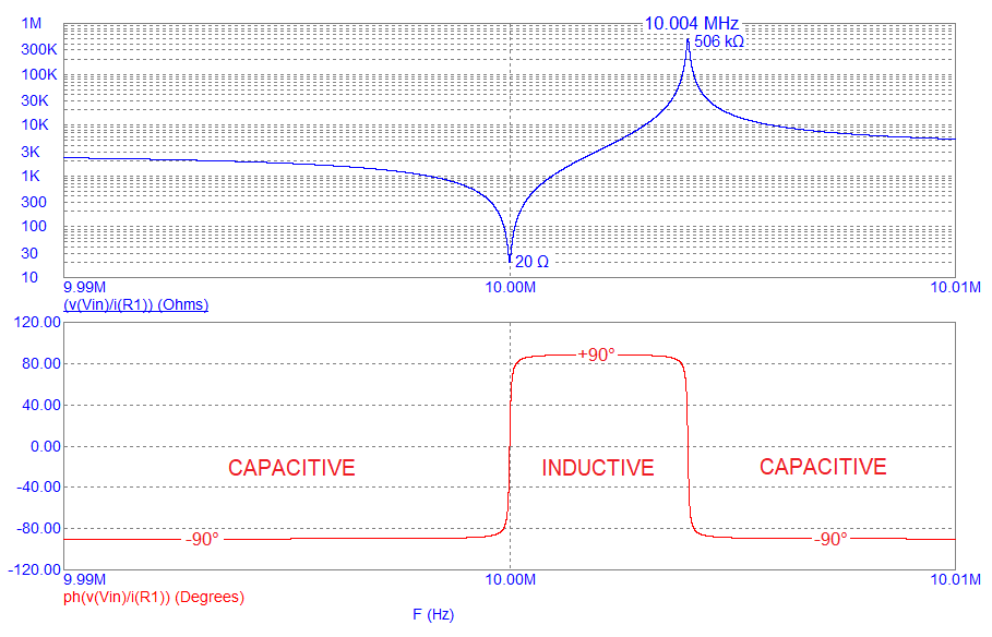
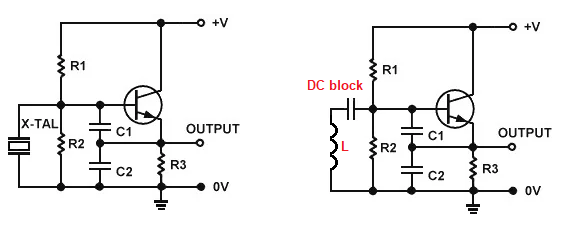
A crystal is expected to present an inductive impedance in this type of oscillator because this is a Colpitts oscillator (specifically a common-collector Colpitts oscillator) and, it requires an inductive component where the crystal is: -

enter image description here

The above is a simulation of a 10 MHz crystal based on average values from various suppliers. The graph is from my basic website and, if you are interested about crystals, that page may be of further use to you. The Colpitts circuit using a crystal is this (to the right uses an inductor): -

enter image description here

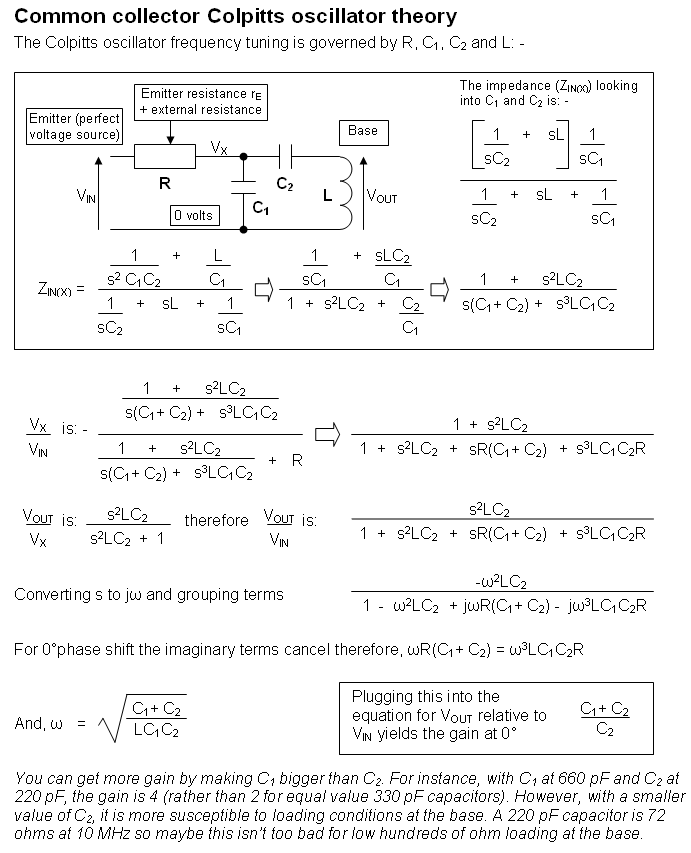
Image from here. So, if you want to know how it works in detail, try googling the Colpitts oscillator type I mentioned and, read until you understand. If there's something that confuses you, come back and raise a new post.

Or maybe this is sufficient: -

enter image description here

\$\endgroup\$
3
  • 2
    \$\begingroup\$ Thank you for pointing out the function of the crystal in this circuit. Most comments before yours forgot to mention the inductive behavior of the crystal and were concerned about second-order effects rather than fundamentals. \$\endgroup\$
    – a360pilot
    Commented Jun 17 at 21:17
  • \$\begingroup\$ I understand the theory reasonably well now, thank you. I have practical issues. The inductor is a crystal, which appears to be fully functional. If I drive it with a function generator, it resonates well at its nominal frequency. I measured the three resistors and both capacitors. All are good. I replaced the transistor and the two capacitors. Still, it does not oscillate. I tried breadboarding the oscillator, but do not have intuitive knowledge to tune it into oscillating. \$\endgroup\$
    – ndemarco
    Commented Jun 23 at 23:04
  • \$\begingroup\$ Why does your circuit use a 100 ohm resistor to bias the base? \$\endgroup\$
    – Andy aka
    Commented Jun 24 at 6:19
6
\$\begingroup\$

When you see the capacitive divider C4/C5, it's usually a Colpitts oscillator or similar. In this case, it's also something like the Clapp oscillator variant. The derivations are a bit lengthy and there's not much point in repeating them here- they're basic knowledge and the Wikipedia page and its references are a good start.

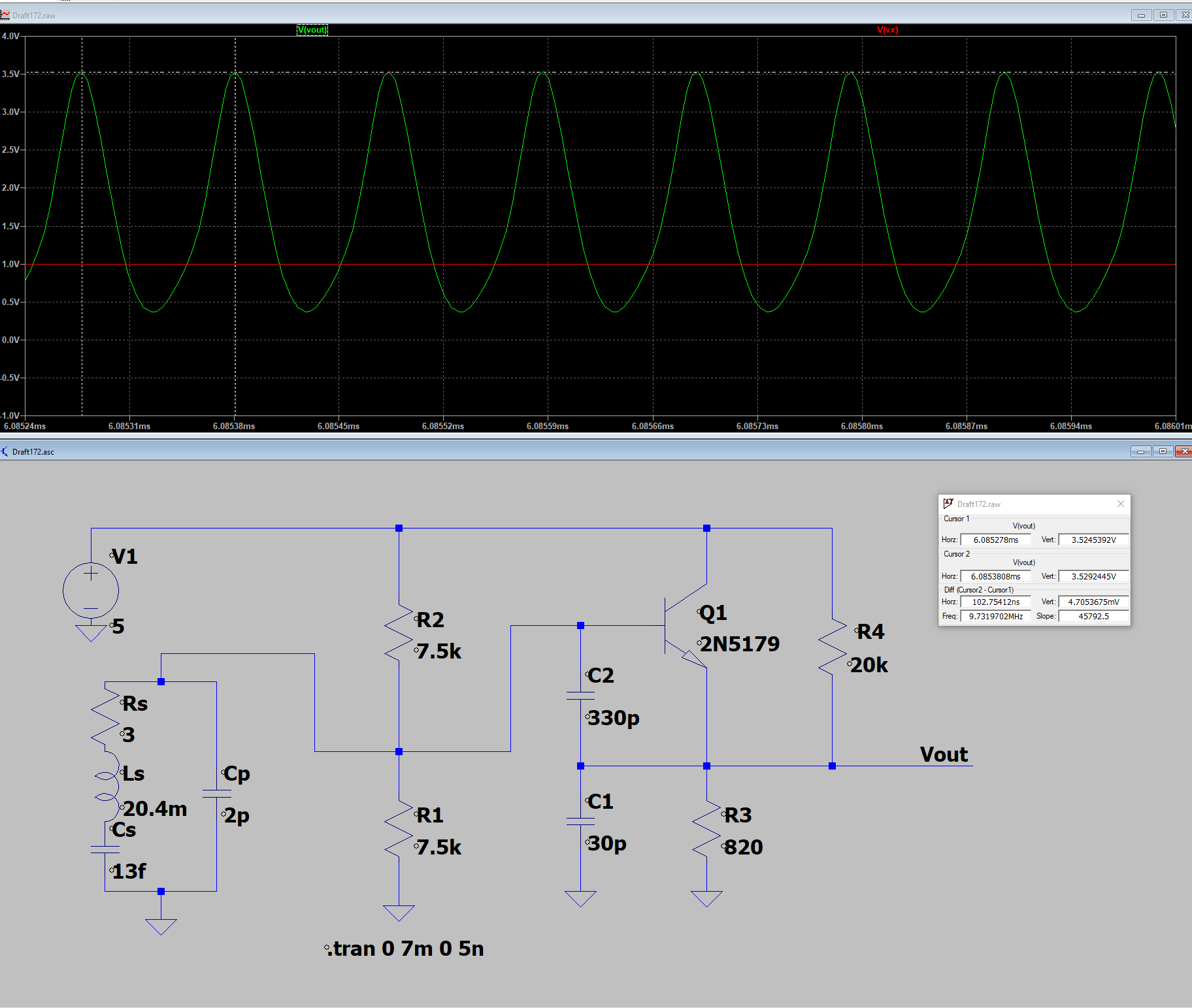
Here's a simulation with a different transistor model. Startup is fairly slow (milliseconds) but it does start and produces a waveform that would switch the LS gate. The 20kΩ load is a (very) rough simulation of the gate input loading.

enter image description here

You can find design equations in Crystal Oscillator Design and Frequency Compensation by Ferking 1978.

\$\endgroup\$
2
\$\begingroup\$

HP85a schematic:

R1&R2 sets the bias point to Vout=Vcc/2-0.7V (in DC analysis).

The crystal creates a DC shifted sine wave voltage across it (AC analysis).

When crystal voltage rises it pushes a current to base but another current (much higher) from C4 pushes also.

Once the C4 is not able to push this current anymore (discharged enough) the output voltage and crystal voltage also start fall. During this fall the C4 is charged.

Then an opposite happens, the C4 is not able to hold the base unsupplied and the output (and crystal voltage also) starts to rise.

\$\endgroup\$
1
\$\begingroup\$

I do not have in my database the BJT 2N3563.
This simulation does not start with some BJT ...

I replaced it with 2N3866 and I got this simulation (short-time simulation).
Note that I did not get what is shown in the Falstad simulator.

Made with microcap v12.
Note that if Rs is greater, the time needed for "starting" may be much longer.

enter image description here

\$\endgroup\$

Your Answer

By clicking “Post Your Answer”, you agree to our terms of service and acknowledge you have read our privacy policy.

Not the answer you're looking for? Browse other questions tagged or ask your own question.