1
\$\begingroup\$

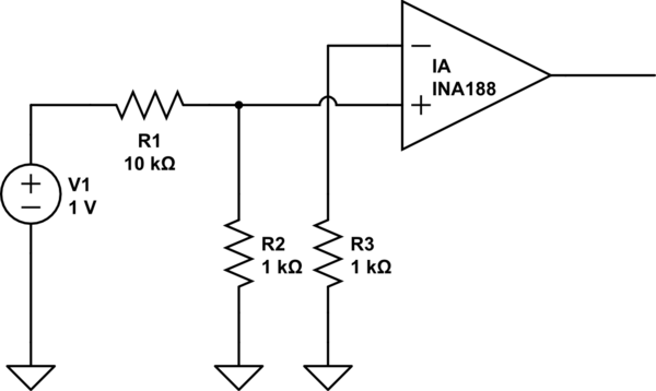
I am trying to understand how the input bias currents flow in op amp and instrumentation amplifier circuits and what errors they create. I came across a circuit that looks like the following:
schematic

simulate this circuit – Schematic created using CircuitLab

My questions are:

  1. If I assume the bias currents flow into the terminals, which way do the bias currents go? For the positive terminal I would assume that the bias current flows from V1 through R1. But what about the negative terminal? Does the bias current flow from ground to the negative input?
  2. What errors do the bias currents create? Is it only the voltage drop across R1 that I need to consider?
\$\endgroup\$
0

4 Answers 4

3
\$\begingroup\$

If I assume the bias currents flow into the terminals, which way do the bias currents go?

Bias currents will flow like this: -

enter image description here

For the positive terminal I would assume that the bias current flows from V1 through R1.

The bias current will split into both paths; R1 and R2.

But what about the negative terminal? Does the bias current flow from ground to the negative input?

Yes it does.

What errors do the bias currents create? Is it only the voltage drop across R1 that I need to consider?

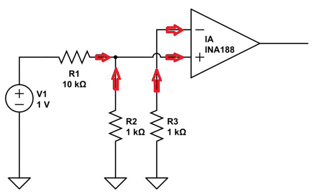
They can create a differential offset voltage that gets amplified by the amplifier and no, you need to consider the volt drops across R1 and R2 together. To make it easier, you can assume the input voltage is zero then, R1 is in parallel with R2 so, the resistive paths on both inputs are clearly different and the bias current will create a differential offset voltage that produces an error.

\$\endgroup\$
9
  • \$\begingroup\$ Thank you for your answer. This is exactly the same as I have read in various articles but i do not understand how the current is flowing from ground to the input. Does it have to do with the input structure of the IA? \$\endgroup\$
    – Robert
    Commented Jun 29 at 16:41
  • 1
    \$\begingroup\$ Yes @Robert, inputs are not perfect, they take a little bit of current even if it's sometimes as low as picoamps. Bias current polarity is normally determined by the amplifier input structure; some will have bias currents that flow into the input pin and some will have bias currents that flow out of the pin but, as rail-to-rail op-amps have come into popularity, you cannot be confident about whether the current flows in or out of the pin. Like I said, it's down to the internal structure of the op-amp/instrumentation-amp. \$\endgroup\$
    – Andy aka
    Commented Jun 29 at 17:03
  • \$\begingroup\$ Ok, understood. Is the case of current flowing into the input only possible for dual supply amplifiers? Because the ground potential has to be higher to source the current, right? \$\endgroup\$
    – Robert
    Commented Jun 29 at 17:11
  • \$\begingroup\$ Yes, if there is no negative supply other than ground, then no current can flow into the pin. But, if the input voltage were maybe a volt higher than ground then the bias current may flow. \$\endgroup\$
    – Andy aka
    Commented Jun 29 at 17:16
  • 1
    \$\begingroup\$ @Andyaka I did miss that, sorry. \$\endgroup\$
    – Hearth
    Commented Jun 30 at 20:11
2
\$\begingroup\$
  1. It depends on the amplifier's input structure: see the data sheet. Bias current refers to the average current into the inputs, so by definition it flows in the same direction for both. The difference is called "offset current".

  2. It produces a voltage offset based on the difference between the resistances the two inputs see. In your case the (-) sees 1k, the (+) sees 1k || 10k ~ 9.09k, a difference of about 90 ohms (assuming perfect resistors). For a max +-2.5 nA, that'll give you an offset due to bias of ~230 nV. You'll never notice that.

\$\endgroup\$
2
\$\begingroup\$

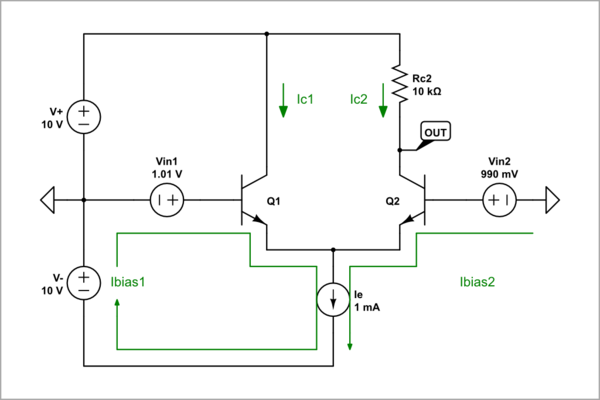
The full path (loop) of the input bias current in the simplified circuit of an op-amp differential input stage below is: the positive terminal of the negative power supply V- >>> ground >>> input voltage source >>> base-emitter junction >>> emitter current source >>> the negative terminal of V-.

schematic

simulate this circuit – Schematic created using CircuitLab

Why did the circuit designers decide to resort to this non-standard solution of closing the biasing current path through the input source? The answer is obvious - in this way they achieved the maximum possible op-amp input resistance because nothing shunts the input.

See more in the links below pointing to related answers of mine:

Why does this op-amp circuit require a resistor to ground?

Why do we need R1 in a non-inverting op-amp?

Need clarification regarding op-amp's ground/ reference and common mode dependence on supply

BJT Differential Amplifier problem

Why put a resistor in series with the positive terminal in a non inverting op-amp circuit?

Designing a differential amplifier

How does the current and voltage stabilize in a differential amplifier?

Un-biasing transistors

See also my question:

Where do input bias currents flow and what voltage drops do they create?

and my answer to it:

\$\endgroup\$
1
\$\begingroup\$

In practice for a single supply amplifier, if the input is GND, the current will flown out from the input. However this doesn't affect the design goal - make the effective resistance at each input equal.

Note this can be achieved by just adding 10 kΩ in parallel with R3 on the example.

In some systems, the added resistors affect slightly the AC performance, and a small C may be added to bypass the DC resistor.

\$\endgroup\$
4
  • \$\begingroup\$ So that means when the bias current is flowing out of the positive input, it is flowing through R1 and R2 too? Not just through R2 to ground? \$\endgroup\$
    – Robert
    Commented Jun 29 at 17:23
  • \$\begingroup\$ I'm curious to know how the input bias current will exit the base of an NPN transistor... \$\endgroup\$ Commented Jun 29 at 17:48
  • 1
    \$\begingroup\$ In a single supply opamp, you can't use NPNs in the input if it handles a common mode to GND. If required the circuit might use NPNs for higher common mode range and PNPs for lower. \$\endgroup\$
    – jp314
    Commented Jun 29 at 18:16
  • \$\begingroup\$ The INA188 uses a chopper based approach to achieve very low offset voltages - the bias current can be positive or negative. The actual circuit arrangement is not shown in the datasheet. As @jp314 states this does not affect the approach used to minimize offset voltages due to bias current. \$\endgroup\$ Commented Jun 29 at 21:39

Your Answer

By clicking “Post Your Answer”, you agree to our terms of service and acknowledge you have read our privacy policy.

Not the answer you're looking for? Browse other questions tagged or ask your own question.