2
\$\begingroup\$

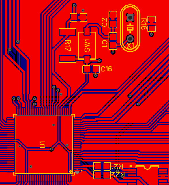
I'm barely getting started with PCB designing. I'm working on my dissertation project and I want to develop a PCB board with an integrated microcontroller (ATmega2560-16AU) and some motor drivers as well. I'm close to finishing the board, but I have some concerns regarding the 16 MHz crystal oscillator that I've added for the microprocessor. Is the layout acceptable?

PCB layout image

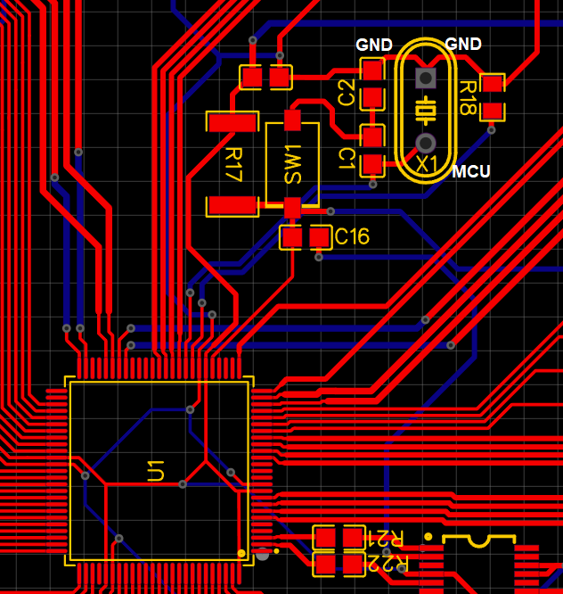
PCB layout image

I've read that the oscillator should be placed as close to the MCU as possible, and I've situated mine at approximately 22-24 mm away. Besides this, I've had to route the traces using several vias (4 at most). Will my MCU's performance be impacted by this design?

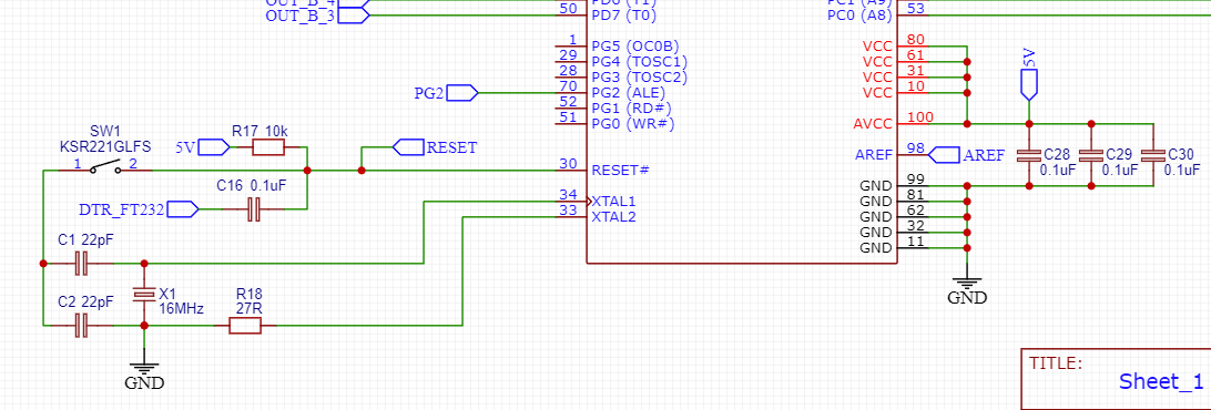
Schematic for the design:

schematic

\$\endgroup\$
5
  • 4
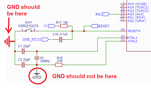
    \$\begingroup\$ You've put the GND connection in the wrong place. It should be at the left-side junctions of SW1 C1 & C2. The bottom junction of the crystal should not be grounded. \$\endgroup\$
    – brhans
    Commented Jul 2 at 12:34
  • 3
    \$\begingroup\$ [ Mod note to the one user who keeps flagging the above comment, saying it's an answer: No, it isn't. It does not answer, nor attempt to answer, the OP's questions about the PCB layout. Instead, it highlights a mistake in the schematic. If that comment had been posted as an answer, people might (understandably) downvote it or flag it as NAA, since it says nothing about the PCB layout, as the question asks. Given that it doesn't answer the OP's question, the only thing it can be is a comment. So it's allowed. Please stop flagging it. TY ] \$\endgroup\$
    – SamGibson
    Commented Jul 2 at 14:59
  • 2
    \$\begingroup\$ Just a point. The crystal is part of the oscillator not the oscillator. The rest of the oscillator is inside the micro. \$\endgroup\$
    – user319836
    Commented Jul 2 at 17:10
  • 1
    \$\begingroup\$ @RussellH: Quite so, and the question is about the layout of the entire oscillator: crystal, loading capacitors, relevant PCB pins, and the traces connecting them. \$\endgroup\$
    – Ben Voigt
    Commented Jul 3 at 16:21
  • 1
    \$\begingroup\$ You definitely have not placed the crystal "as close to the MCU as possible". Notably, there's a fat reset switch circuit occupying the space in between -- the reset switch is very low frequency, and does not need to be close. Easy win just by swapping the crystal and reset locations. \$\endgroup\$
    – Ben Voigt
    Commented Jul 3 at 16:23

3 Answers 3

6
\$\begingroup\$

No it is not acceptable, the crystal needs to be close to the pins to minimize EMI. In this case I believe the pins are named XTAL1 and XTAL2. From each pin you should have as short a trace as possible to each side of the crystal.

If you read the friendly application notes for this part, Microchip has even given out a free AVR186: Best practices for the PCB layout of Oscillators .

Apart from that I don't understand the circuit.

  • C1 and C2 should both be directly grounded. You placed C1 in series with ground from C2's point of view.
  • R18 is often not necessary for simple oscillators like this, but if you want one for tuning purposes you could place a 0 ohm resistor there.

Other remarks not related to your question:

  • C16 should be grounded. Why is there a signal in series with it?
  • There will be protection diodes inside the MCU, but best practices is still to place something SW1 in series with a resistor like 100R towards the MCU, for the simplest form of ESD protection.
  • Given the 2 layer layout, it is fishy that you've routed all VCC pins together before the decoupling caps. The caps should be close to the respective VCC pin or they won't do you as much good.
\$\endgroup\$
4
  • 1
    \$\begingroup\$ +1 to the answer. The only thing I'd add is that since you're using surface mount for everything else you probably want to use a surface-mount crystal. If nothing else, this will make it easier to put the crystal close to the microprocessor body. The only reason not to is if you're concerned about overdriving the crystal: I'd consult the data sheet and any applicable app notes to see what the manufacturer has to say about their oscillator pins: there should be instructions. \$\endgroup\$
    – TimWescott
    Commented Jul 2 at 14:12
  • \$\begingroup\$ @TimWescott Oh yeah I didn't notice that. Also I think we are past the time when HC49 (SMD or not) was the cheapest package. So maybe they should consider using a flat low profile one while they are at it. The SMD HC49 is kind of notorious of ending up with poor wetting during reflow, especially if the pad layout is so-so. \$\endgroup\$
    – Lundin
    Commented Jul 2 at 14:20
  • \$\begingroup\$ Thanks for the prompt answer! I'll change the layout so that the oscillator is closer to the mcu. But it's gonna be more difficult considering that i have a number of pins that I'm using around the XTAL1 and 2 area. Would it be a bad idea to rout some of them using via's beneath the microprocessor? \$\endgroup\$
    – hdaniu
    Commented Jul 2 at 15:01
  • 1
    \$\begingroup\$ @hdaniu When doing PCB design start with the most sensitive parts and then everything else has to adapt. The common way is to let the crystal sit next to the MCU and any pins nearby will have to make their merry way from there through vias etc indeed. So that's one more reason to use 4 layer stackup apart from better ground. \$\endgroup\$
    – Lundin
    Commented Jul 2 at 15:46
5
\$\begingroup\$

Is the layout acceptable?

You should use a full ground plane for this type of design. It cost pennies to make your PCB 4 layer from 2 layer and will save you hours of messing around trying to locate oddball problems but, having said that your schematic is incorrect around the crystal: -

enter image description here

I'm not ruling out other problems.

\$\endgroup\$
6
  • 3
    \$\begingroup\$ +1 for the 4 layer advise, there's really no reason to use any 2 layer stackup for MCU boards these days, if there ever was one. \$\endgroup\$
    – Lundin
    Commented Jul 2 at 11:57
  • 1
    \$\begingroup\$ Suggesting a 4 layer board for a measly 16 MHz MCU is a bit weird. If going for a 4 layer board, you might as well suggest to replace the 16 MHz 8-bit ATMega2560 with a 500 MHz 32-bit ARM MCU with megabyte of RAM and Flash and it would still be in fact cheaper. \$\endgroup\$
    – Justme
    Commented Jul 2 at 13:29
  • \$\begingroup\$ @Justme I don't think you can possibly say that given that the OP hasn't disclosed the full details of the circuit board. He does say it's a board with an integrated MCU but he also hints at other things including motor drivers. So, this isn't a 4 layer board for a just measly 16 MHz MCU is it. \$\endgroup\$
    – Andy aka
    Commented Jul 2 at 13:46
  • 1
    \$\begingroup\$ @hdaniu a 4 layer board is easier to lay out, has better EMI performance and costs only a little bit more than a 2 layer board. \$\endgroup\$
    – Andy aka
    Commented Jul 2 at 16:25
  • 2
    \$\begingroup\$ @Justme It's not really related to signal speed as much as easier routing of QFP signals. Also it is kind of rare to see a board without a switch regulator these days and it's not easy to get a proper switch regulator design with just 2 layers. But yeah they really ought to move away from these old crap MCUs to ARM since there's about as few reasons to use 8-bitters as there is to use 2 layers. Writing C code for 8-bitters is kind of analogous to routing manual ground traces and using LDOs: crude, cumbersome, yesterday's technology. \$\endgroup\$
    – Lundin
    Commented Jul 3 at 6:42
1
\$\begingroup\$

The whole reset/crystal circuitry is wrong so it won't even work.

Please look at data sheet or hardware getting started guide appnote or even look at the Arduino board schematics you seem to have copied.

While some people have commented about the layout needing improvements, it is true that most appnotes how to make the routings for crystal show much better layouts, but I would say that if you fix the schematics and fix the PCB wiring accordingly, the PCB layout for 16 MHz AVRs is usually the least problem you have to worry about.

People tend to run these kind of AVRs on breadboards and sometimes without proper decoupling caps, so you seem to have the basics covered.

I'd say the layout could be much better and the crystal could be much closer to MCU for much shoter wiring without no vias, but it should still be acceptable as in there is likely no issues having the crystal within 1 inch of the MCU.

Edit: It looks worse than what it is - you simply have misplaced the ground symbol to wrong side of the capacitor so it is a small schematic fix.

\$\endgroup\$
1
  • \$\begingroup\$ Thank you guys for your answers! I've actually just noticed that something was fishy when I was screenshotting my schematic. I don't know why I fudged up my ground connections like that, but I've modified them. \$\endgroup\$
    – hdaniu
    Commented Jul 2 at 15:05

Your Answer

By clicking “Post Your Answer”, you agree to our terms of service and acknowledge you have read our privacy policy.

Not the answer you're looking for? Browse other questions tagged or ask your own question.