6
\$\begingroup\$

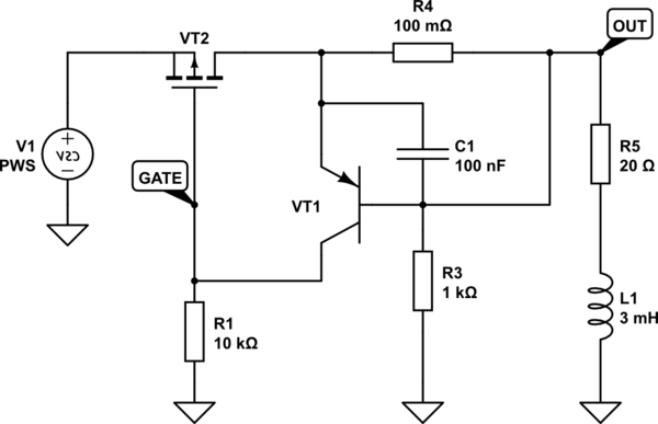
Here is a circuit designed to protect a load (an incandescent lamp) from short circuits. It is supposed to work as follows: VT2 is initially conducting — its gate is pulled to ground through R1. A voltage close to 12 V is applied to the base of VT1 (marked “out”) and keeps it off. Capacitor C1 charges through R3.

In case of a short circuit (the resistance of R5 suddenly drops close to zero), the potential at “out” sharply decreases, which turns on VT1, and a potential of about 12 V is applied to the gate of VT2, turning it off.

Please let me know if this circuit will work. I feel like I'm missing something important.

And of course, I would be happy to hear any suggestions for improving the circuit.
schematic

simulate this circuit – Schematic created using CircuitLab

\$\endgroup\$
12
  • \$\begingroup\$ It depends how you define "work". Have you simulated the circuit to see if it "works" like you expect or not? \$\endgroup\$
    – Justme
    Commented Aug 5 at 11:33
  • \$\begingroup\$ @Justme Yes, I have simulated this in Qucs, and overall, I am satisfied with the results. By "works," I mean disconnecting the power from the load after a sudden decrease in load resistance. I simulated the transient process, using a single pulse source instead of a constant voltage source. Overall, everything looks good, but I decided to show the circuit to the community to see if there are any things I might not be aware of. \$\endgroup\$
    – RUMBUFDSI
    Commented Aug 5 at 11:46
  • 4
    \$\begingroup\$ how is the load being protected? ... protected from what? \$\endgroup\$
    – jsotola
    Commented Aug 5 at 15:05
  • 6
    \$\begingroup\$ Why would an incandescent lamp need protection from a short circuit (it would turn off) or from incorrect polarity (incandescent lamps have no polarity and light up both ways)? \$\endgroup\$
    – Justme
    Commented Aug 5 at 16:17
  • 1
    \$\begingroup\$ What is the inrush current for a cold incandescent bulb's filament? Will it look like a short circuit to your protection circuit? \$\endgroup\$
    – Sotto Voce
    Commented Aug 6 at 6:51

6 Answers 6

14
\$\begingroup\$

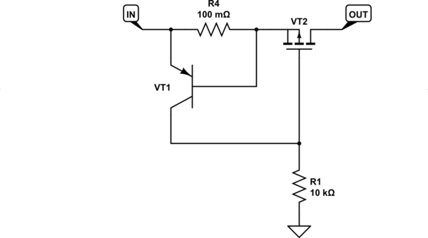
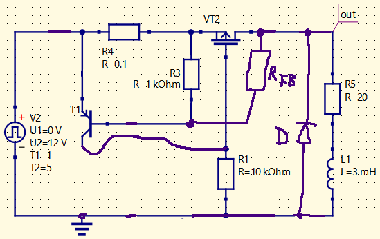
You're on the right track, but as soon as drain voltage drops a bit, the BJT can't really pull off the PMOS anymore, can it?

Put it "in front" instead. This makes the traditional "ring of two" current source. PMOS must be large and well heatsinked, since it'll be dropping a good 6A -- at 12V, that's 72W short-circuit!

enter image description here

The capacitor and other pull-down resistor aren't necessary (R3 is simply in parallel with the load, and C1 doesn't do much paralleled by R4, or more to the point, its value has to be quite large to do much of anything), however you can make a divider between current sense, base and output (Rfb into R3) that helps turn off VT2 as its voltage drop increases -- this is called foldback current limiting.

Since you show an inductive load, then if V2 will be switched, or VT2 by additional wiring to this circuit, consider adding D to protect against drain voltage avalanche.

Note that foldback gives the output a negative-resistance characteristic, i.e. current falls as voltage (across VT2) rises. This will oscillate with an LC load (the load is shown as inductive, but wiring capacitance, or the transistor itself, can serve as the capacitance). It would be prudent to place an R+C series snubber, say where D is (in parallel with it), with C > 3 times the expected transistor, diode and wiring capacitance (or just make it fairly large because who cares, 100nF say), and R < -negative resistance (probably 1-2 ohms would suffice).

\$\endgroup\$
8
  • 2
    \$\begingroup\$ +1 for the answer and the excessive work on the existing image. One other thing worth to note is the reverse polarity: VT2's body diode will be forward-biased (ignoring the D diode in your circuit) so the incandescent bulb will still light up but there won't be any current limiting or S/C protection. \$\endgroup\$ Commented Aug 5 at 12:52
  • 1
    \$\begingroup\$ This answer is extremely helpful, thank you very much! \$\endgroup\$
    – RUMBUFDSI
    Commented Aug 5 at 12:57
  • 1
    \$\begingroup\$ @RohatKılıç Check again -- it's PMOS, source to V2. The arrow shows the substrate diode pointing up. \$\endgroup\$ Commented Aug 5 at 13:09
  • 1
    \$\begingroup\$ @TimWilliams yes, it's PMOS. The body diode's cathode at S, anode at D. In case of a reverse-polarity input it'll be forward-biased (again, ignored the diode D in your schematic). Though the OP said a reverse-polarity protection is implemented in an early stage but what if there wasn't any. \$\endgroup\$ Commented Aug 5 at 15:03
  • 2
    \$\begingroup\$ The the question says 12V and made no concerns about reversal, cross-wiring, etc., so are not a concern. For example, it might be supplied from a (hard wired) battery or SMPS, or be part of a larger module where the 12V is by design, or already protected against such, etc. It's a building block, not a complete standalone module. That's how I understood the question. \$\endgroup\$ Commented Aug 5 at 15:30
11
\$\begingroup\$

The circuit you show is a current regulator, not a fuse. Once the output is shorted, VT2 is controlled to limit the current at about 5-6A, and it will dissipate accordingly (>60W), as long as the short circuit is present. It will quickly overheat and get destroyed.

Instead, you'd probably want a circuit that latches into the OFF state. To reset it, the power must be removed then reapplied, after the short circuit was removed of course.

schematic

simulate this circuit – Schematic created using CircuitLab
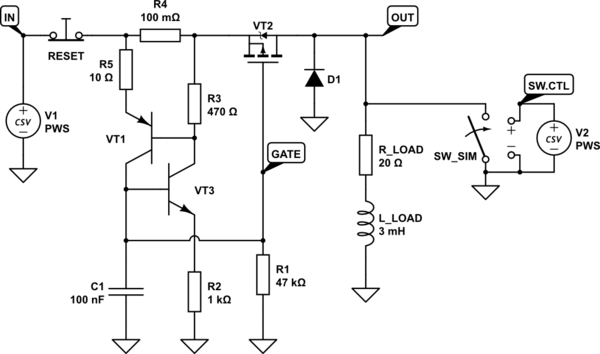
R4 is the current sense resistor, R3-VT1 detect the excessive current, VT3 latches VT1 once it starts turning on. R2 limits the SCR ON current. C1-R5 add rudimentary immunity against transients. D1 protects against negative spikes generated by the load inductance.

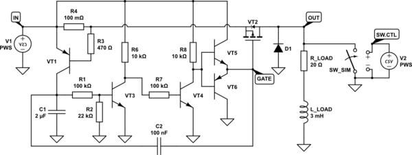
Instead of a permanent latch, we can turn the load off for some fixed duration, then turn it back on - and off again if the short persists. This can be done with a monostable.

schematic

simulate this circuit

VT3 and VT4 are inverters. The 2nd inverter's output is buffered from C2 and VT2's gate capacitance by the buffer VT5 and VT6.

C2 adds positive feedback that speeds up the output transitions of the latch.

To prolong the off time, increase C1 and C2 by the same factor, e.g. both by 5x, etc.

\$\endgroup\$
2
  • 3
    \$\begingroup\$ You could also use a thyristor for the latch. I have seen that in old circuits, like in a pump controller to tay shut off until the supply is switched off and on. \$\endgroup\$
    – Boldar
    Commented Aug 6 at 13:08
  • 2
    \$\begingroup\$ @Boldar Of course. I was just making a thyristor from discrete transistors as is my fancy when using CircuitLab :) \$\endgroup\$ Commented Aug 6 at 14:38
6
\$\begingroup\$

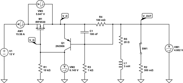
If you continue your analysis you will see, that during a shortcut of the output, closed SW1 here, the circuit enters a half conducting state of M1, where more than 90W will be dissipated.

When Q1 starts conducting, indeed the gate voltage of M1 and the current is reduced, but this also reduces Vbe of Q1. This is a metastable situation until M1 burns away, except this high power loss is intended and proper cooling is established.

schematic

simulate this circuit – Schematic created using CircuitLab
\$\endgroup\$
2
  • \$\begingroup\$ Yes, now I see the problem, thank you! But if I connect the emitter of VT1 to the 12V supply not after VT2, but before it, that is, directly to the "+" of the power source, will it work? \$\endgroup\$
    – RUMBUFDSI
    Commented Aug 5 at 12:28
  • 1
    \$\begingroup\$ No, then you have the voltage across M1 also across B-E junction of Q1 and so Q1 will sublime immediately. \$\endgroup\$
    – Jens
    Commented Aug 5 at 17:00
5
\$\begingroup\$

To confirm what @Jens was saying, here is the "utility" curve of the "protection"...

You can see why the "protection" is not "very effective".

enter image description here

you should add a pair of BJT (Q1 & Q2 = SCR) like these, more effective.
Q4 is not very "useful" (only affected by temperature).

enter image description here

\$\endgroup\$
1
  • \$\begingroup\$ Thank you very much for your help! I have already considered this circuit in my previous questions. It works, but I wanted to try making a circuit with fewer components. \$\endgroup\$
    – RUMBUFDSI
    Commented Aug 5 at 13:14
4
\$\begingroup\$

Depending on \$R_{DS}\$ of VT2 when fully switched on, and the robustness of VT1's base-emitter junction, under an output short-circuit condition you might find the system in a state like this:

schematic

simulate this circuit – Schematic created using CircuitLab
The potential at VT2's drain, node D, is very low. Transistor VT1, which is responsible for raising VT2's gate potential, can never raise it above D. It would need to apply closer to +12V to VT2's gate (so that \$V_{GS}\approx 0V\$) to switch it off, but it can't.

Transistor VT1 and sense resistor R1 should be on the source side of VT2, so that it's always possible to apply the fully supply potential to VT2's gate:

schematic

simulate this circuit

\$\endgroup\$
3
\$\begingroup\$

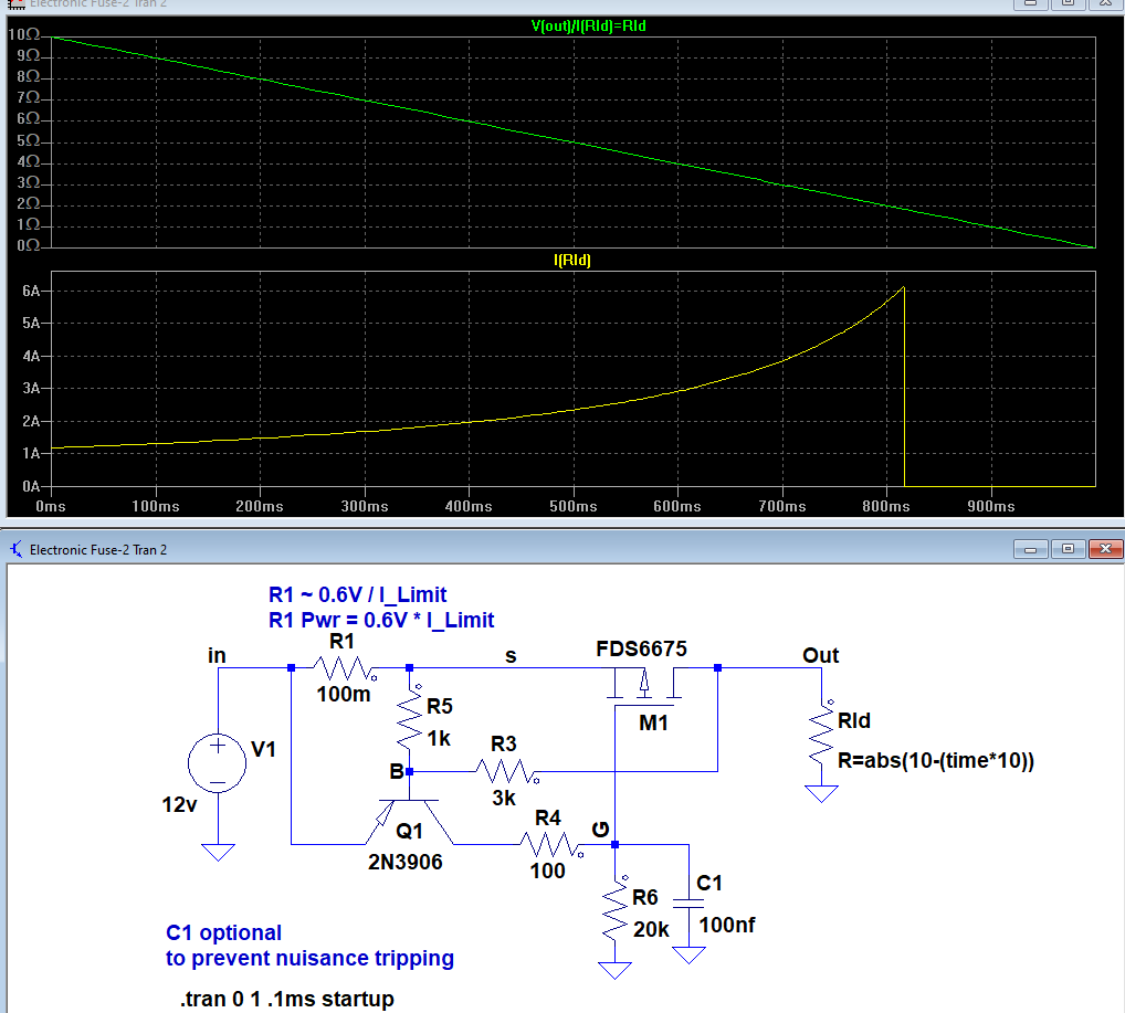
Below is the LTspice sim of a simple electronic fuse circuit using just 1 PNP BJT and 1 P-MOSFET.

For R1 = 100mΩ, it triggers at about 6A current through the load, with the load current then dropping to zero (yellow trace). At no time is there significant steady-state power dissipated in the MOSFET, other than from the load current times the MOSFET on-resistance.

It is reset by removing the short.

enter image description here

\$\endgroup\$
1
  • 3
    \$\begingroup\$ Beware the capacitor to gate -- it may be prone to high-frequency oscillation during transition, especially if the In/s path is unknown (read: potentially inductive; really, even mere inches of trace length could be problematic here). It also makes the MOSFET susceptible to damage on inrush (if the 12V supply may be hot-plugged, especially through a long cable, or if using the design at higher voltage). \$\endgroup\$ Commented Aug 5 at 16:49

Your Answer

By clicking “Post Your Answer”, you agree to our terms of service and acknowledge you have read our privacy policy.

Not the answer you're looking for? Browse other questions tagged or ask your own question.