0
\$\begingroup\$

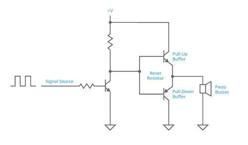
enter image description here

Source : https://www.allaboutcircuits.com/industry-articles/an-overview-of-driver-circuits-for-piezo-transducer-buzzers/

The transistors are MJE340 and MJE350 and NPN and PNP pair. I am using these since I need to be able to switch a good 100- 120.

I intend this stage to feed a LC filter to make the whole thing a class D amplifier, I want to pass a 33kHz PWM that will be demodulated through the filter.

to start with I send 50% duty cycle square wave through the input, I've noticed the following while reading the voltage at the emitter end.

  1. The 'ON' time reduces with increased frequency, gradually reducing and turning close to a pulse/impulse around 15kHz and then disappearing altogether.

  2. The greater the collector resistor on the first stage, the worse the above effect gets even at even lower frequencies.

  3. Removing DC (Voltage was 0 to 5 volts DC) offset at the signal (voltage -2.5 to + 2.5) seems to fix the problem and I can see 50% duty cycle square wave all the way till 55kHz. This works but I'm not sure how to accomplish this, not sure a coupling capacitor at the base would do the trick since I don't quite see a way for it to discharge through the PN junction at the base.

What would best explain this behavior and what can I do about this?

Using this as a haptic actuator, it's a PowerHap 1919 and the source voltage goes all the way up to 120 volts max. I intend this as a class D amplifier, I have an LC low pass filter that works well enough with the actuator. If only I could get a 100 volt PWM signal into that, all would be good.

\$\endgroup\$
6
  • 1
    \$\begingroup\$ Vrisk, You will need a much more crafted design than that one! You will also likely requires "speed ups" to be included in order to forward ahead the rising and falling edges to the output stages. If you want things to work well at 55 kHz (not difficult, but starting to push things a bit), then these details start to matter. I have a circuit template that will work very well at that frequency and deliver a good 50% duty cycle with approximately equal rising and falling edge times. But this isn't entirely a walk in the park, either. And you will need to avoid solderless breadboards. \$\endgroup\$ Commented Aug 20 at 16:09
  • \$\begingroup\$ @periblepsis what speedups ? Yeah send the circuit if you can, I'll try to understand better whats going on and what the differences are. I thought the breadboard might be the problem and I moved to a perf board, the problem didn't change much. \$\endgroup\$
    – Vrisk
    Commented Aug 20 at 17:31
  • \$\begingroup\$ Tell me the buzzer model and make. And may I assume this is a buzzer and not a speaker for music or voice? Also, what is the source voltage and its output impedance? \$\endgroup\$ Commented Aug 20 at 18:15
  • \$\begingroup\$ @periblepsis not really using this as a buzzer but as a haptic actuator, it's powerhap 1919 and the source voltage goes all the way upto 120 volts max. I intend this as a class D amplifier, I have a LC low pass filter that works well enough with the actuator . If only I could get a 100 volt PWM signal into that, all would be good. \$\endgroup\$
    – Vrisk
    Commented Aug 20 at 18:33

3 Answers 3

2
\$\begingroup\$

The duty cycle changing is explained by the asymmetric first stage. It just is not visible at low frequencies.

You have strong fast transistor that pulls signal down hard and fast with large sinking current. But only a resistor for sourcing current.

It means that the first stage can pull low fast but pushing high is slow.

It may be worsened by the fact how the first stage is driven, but assuming it is a logic level square wave from MCU or signal generator, the base drive turns the first stage transistor on hard, but it takes time to turn it off through the same resistor.

You can improve the driving of first stage by adding a diode which speeds up turning off the first stage.

In general, you might want to replace the whole thing with a level-shifting FET driver, a single IC that's capable of driving the second stage or even the speaker directly.

Edit: There's two ways of connecting a speedup diode - one is to put in in parallel to speed up discharge of current out of base even though it still saturates hard, but the other more effective way is a Baker Clamp between base and collector to prevent the transistor from saturating hard to begin with.

Also like I mentioned, whatever is after the first stage, you can see that the first stage transistor is strong and fast, it can discharge any charges in the load fast, sort of like think replacing it with a zero-ohm pushbutton. But when you release the pushbutton, whatever there is on the output, the drive and charging current is limited to slow speed by the resitor to positive voltage. Turn-on will be much slower than turn-off because turn on happens via some arbitrarily high resistance and turn-off happens via some arbitrarily low resistance.

So the first stage causes already duty cycle problems because both how it's input is driven and how it's output drives the next stage lengthens the low output.

\$\endgroup\$
6
  • \$\begingroup\$ I don't follow, I encountered a similar problems with asymmetry like one you described while trying to drive current through a coupling capacitor and an NPN transistor without a push pull stage, I don't quite see what's going on here though. My understanding is when the first stage transistor is off, then it saturates the second stage regardless of the current sent in so the asymmetry wouldn't matter. further I don't understand is how removing the DC offset makes this problem better. Also what's 'level shifting ' ? \$\endgroup\$
    – Vrisk
    Commented Aug 20 at 17:41
  • \$\begingroup\$ also where do I put that diode and how would that help ? \$\endgroup\$
    – Vrisk
    Commented Aug 20 at 17:48
  • \$\begingroup\$ Your response was the closest to answering my question, I'd appreciate it if you could elaborate a bit more. \$\endgroup\$
    – Vrisk
    Commented Aug 21 at 3:12
  • \$\begingroup\$ @Vrisk There. For terms such as "level shifting" or "transistor speedup diode" you likely can find explanations faster for concepts you are not familiar with if you do a google search than wait someone to answer your question. Wikipedia is a great resource if you don't have a practical electronics textbook. \$\endgroup\$
    – Justme
    Commented Aug 21 at 4:39
  • \$\begingroup\$ I think I'm seeing it more clearly now, but you seem to be talking about charging the base of the transistor almost like charging a capacitor. Is there any way I can predict the change in duty cycle given a certain collector resistance? Some kind of RC time constant kind of thing perhaps? \$\endgroup\$
    – Vrisk
    Commented Aug 21 at 4:47
2
\$\begingroup\$

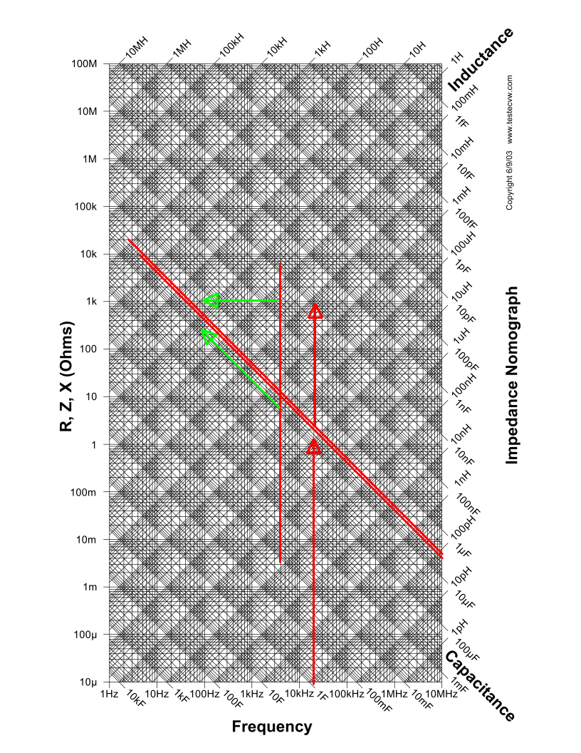
You cannot design anything without an accurate model of the load. In this case, the load of the 1919 Haptic Piezo device is 2.5μF with an SRF (resonance) of 15 kHz so 20 kHz is beyond spec. and 10kHz may be a practical limit for thermal reasons depending on the power applied.

To see the impedance curve for 2.5 uF vs f follow the curve and your switch must be at most 5% of the impedance of the load for efficiency. It is easier just to use a 10A half-bridge CMOS switch if you plan on pushing the limits.

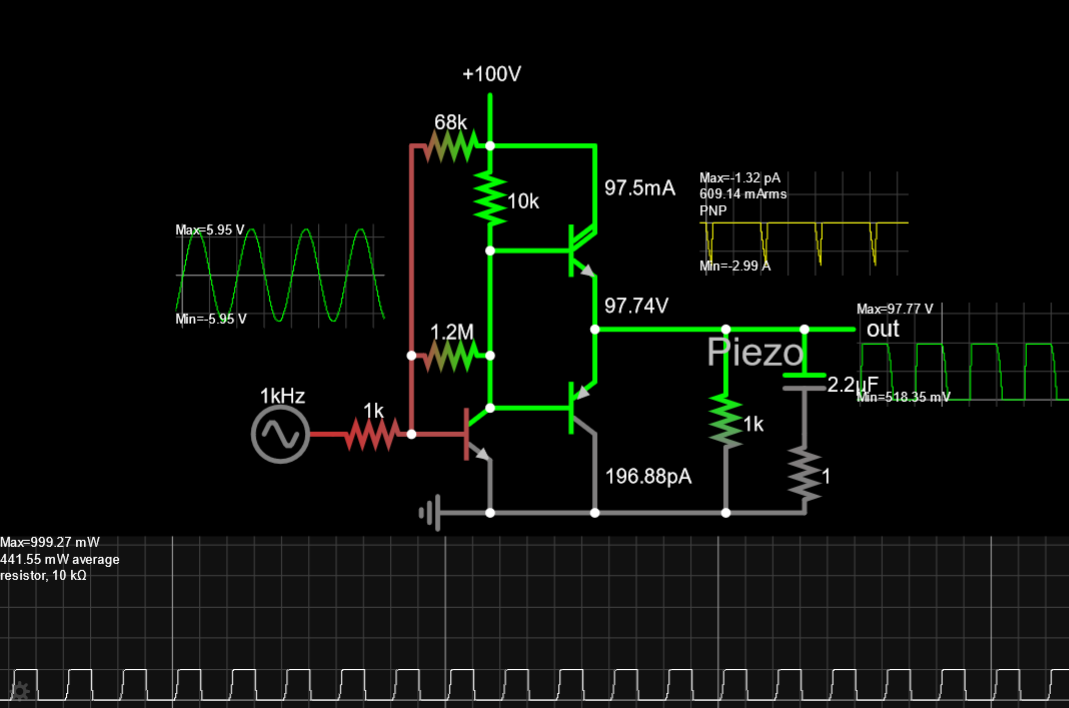
enter image description here

My suggested circuit design uses a sine or square drive, polar or bipolar with small adjustments to bias 12Vpp. Negative feedback gives better duty cycle symmetry with correct DC bias and more BW with lower gain. R.base will change with input drive level.

I assumed a 100Vdc supply and 2.2uF low ESR Piezo load with a Darlington NPN and I assumed hFE = 10 for the input NPN for Ic/Ib=10.

enter image description here

Conclusion

The OP's design goals need to no exceed the device specs.

Maximum operation frequency The operation frequency is limited by the self-heating of the component, which should not exceed +30 °C. This is reached after about 10 s of continuous square signal 0 ... 120 V at 500 Hz Maximum voltage change rate 1.2 MV/s

\$\endgroup\$
1
\$\begingroup\$

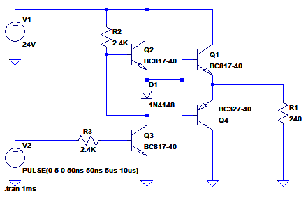
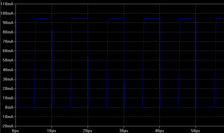
Try this circuit. It can easily drive close to 100mA into the load with only small duty cycle degradation at shown pulse drive frequency of around 100kHz.

Driver Circuit

Current into load

\$\endgroup\$
7
  • \$\begingroup\$ What's Q2 and D1 doing with the base tied to the emitter that way ? \$\endgroup\$
    – Vrisk
    Commented Aug 20 at 19:40
  • \$\begingroup\$ 240 Ohms is the wrong load for the 1919 Haptic. (not your fault, as it wasn't specified by OP) \$\endgroup\$
    – D.A.S.
    Commented Aug 20 at 19:52
  • \$\begingroup\$ @Vrisk - Q2 acts as an active pullup to provide lots of high side drive. The diode D1 produces a forward voltage drop when the lower NPN Q3 turns on. This forward voltage reverse biases the BE junction of Q2 which very quickly turns it off. \$\endgroup\$ Commented Aug 20 at 19:59
  • \$\begingroup\$ That's very very nice, I get it now. I probably just go with this, it's simple and effective. Where did you get that 100mA number from? also do the values of R2 and R3 really matter, I'd like keep them high to deal with the fact 100 Volts will be passing through R2 when Q3 turns on \$\endgroup\$
    – Vrisk
    Commented Aug 20 at 20:22
  • \$\begingroup\$ @Vrisk - You will have to select resistor values that suit your application and power supply voltages. You will also need to select transistors that have compatible voltage and current ratings. I used LTSpice to simulate the circuit and presented here mostly to show as a circuit concept. \$\endgroup\$ Commented Aug 21 at 2:01

Your Answer

By clicking “Post Your Answer”, you agree to our terms of service and acknowledge you have read our privacy policy.

Not the answer you're looking for? Browse other questions tagged or ask your own question.