1
\$\begingroup\$

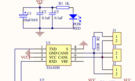
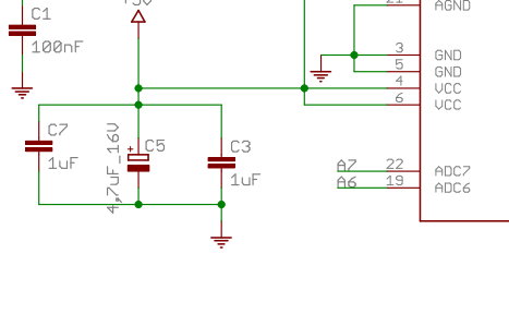
I am trying to make a PCB of a Arduino circuit, this involves MCP2515 CAN Module and Arduino NANO and a DAC. When I saw the schematics of all the three break out boards I see that all have decoupling/filter capacitors.

My question here is that can remove all of these capacitors provided my buck module output power supply is good enough?

Arduino NANO capacitors https://www.arduino.cc/en/uploads/Main/Arduino_Nano-Rev3.2-SCH.pdf

CAN Module capacitors https://www.tronisoft.com/store/MCP2515-CAN-Bus-Driver-Module-Board-TJA1050-SPI-MCU-Arduino

\$\endgroup\$
3
  • 1
    \$\begingroup\$ Do you realize that the bypass capacitors must form a tight loop from VCC to GND pins to be effective? If so, how would you simultaneously have the same capacitor effectively bypassing two devices in different places at the same time? \$\endgroup\$ Commented Aug 21 at 14:04
  • 1
    \$\begingroup\$ Siddharth Hiremath - Hi, Where did the images come from? To comply with the site rule on referencing, details of the original source of copied / adapted material must be provided by you, next to each copied / adapted item. If the original source is online & public, please edit the question & add the webpage/PDF name & its link (URL) (e.g. website name + webpage title + its URL). If the source is offline (e.g. book or private intranet) then edit the question & add full source details e.g. title, author, page, publisher, edition. (More site rules in the tour & help center.) \$\endgroup\$
    – SamGibson
    Commented Aug 21 at 14:38
  • \$\begingroup\$ Sprinkling 0.1uF decoupling capacitors around the board is already such a huge "this should be good enough" rule of thumb, no one can answer this definitively. These capacitors are so cheap as to effectively be free. My advice? Put one as close as possible to each Vcc pin on every IC and move on. \$\endgroup\$
    – spuck
    Commented Aug 21 at 22:33

4 Answers 4

11
\$\begingroup\$

Likely no, you cannot remove all the capacitors.

The bypass capacitors are for local storage and they must be near the IC to work properly, so that when an IC needs a burst of energy, the local capacitor can provide it fast instead of wiring inductance causing a drop in the voltage while energy comes from a capacitor that is farther away.

The larger bulk capacitors can be further away. You likely don't need all the large bulk capacitors.

\$\endgroup\$
4
\$\begingroup\$

Generally: no, these caps should be placed as close to the MCU supply pins as possible. So there may be multiple caps because there are multiple supply pins. Decoupling does not just serve to remove conducted emissions (although that's the main purpose) but also radiated emissions picked up by traces or components on your PCBA. Which is particularly likely to happen if the part sits next to some wireless device.

As for 1uF that's somewhere in between "bulk caps" meant to keep the supply stable and "decoupling caps" meant to remove high frequency EMI. But they could also (less likely) serve the purpose of removing EMI coming out from inside the MCU or other IC, particularly if there's built-in regulators.

The rule of thumb is to follow manufacturer recommendations. Just looking at the schematics isn't very helpful either since the physical location of the cap is what matters. If lots of decoupling caps with similar values are placed physically very close to each other (<10mm), then that's probably a waste and some could be removed.

Larger bulk caps are typically placed together with the voltage regulator where the board supply enters the PCBA. This design looks a bit aged/naive since it proposes polarized tantalum caps for bulk caps. But at 10uF 16V or lower you wouldn't pick tantalum caps these days, because they are expensive and error-prone, to be avoided when possible. These days 10uF is widely available in ceramic caps - at 16V probably somewhere around 0805 to 1210.

But then of course MCP2515, TJA1050 etc is 20+ years old vintage electronics as well...

\$\endgroup\$
2
  • 2
    \$\begingroup\$ Also note that in case of some dysfunctional 2 layer design, you'll likely need much more caps than a 4 layer design with a dedicated ground plane. \$\endgroup\$
    – Lundin
    Commented Aug 21 at 14:20
  • \$\begingroup\$ Thanks a lot foe the detailed explanation, really appreciate that! \$\endgroup\$
    – Sid
    Commented Aug 23 at 17:24
3
\$\begingroup\$

Possibly yes. It depends.

Capacitors are provided for local bypass purposes. Don't let the schematic fool you: they are often collected off to one side for convenience, but are meant to be placed adjacent to respective / important / priority components that need them.

If major components will be placed together, they can likely share bypass capacitors. When the currents through each device's power pins are orthogonal, uncorrelated, they don't impact each other and the ripple voltage seen at each device's supply pins are largely due to their own current draw; and with enough capacitance for the worst/heaviest load on that supply, the corresponding ripple voltage remains nominal.

Notice what's going on here: a device has some dynamic current consumption, which creates a dV/dt in the nearby capacitor, and draws current through nearby traces (which are small inductors), and so on up the chain. The study of this is PDN (power distribution network) analysis. I won't go into further detail here, but suffice it to say, there is a way to calculate what is needed and where.

AVR MCU and CAN controller aren't especially fast or powerful devices, and I would expect they can share bypass caps when placed within a couple cm of each other. Currents may or may not be correlated (depends on CAN clock source/settings). The CAN interface/PHY is a far stronger load and will need a bit more capacitance for itself.

The MCU in and of itself isn't very powerful, but if you have many strong loads attached (e.g. LED display?), mind the total current through GPIOs -- you see, how the analysis depends on so many things?

If you aren't doing the analysis, the safer plan (but, still not guaranteed: there are potential problems this way too) is to keep capacitors local to each device, to keep all power pins well supplied.

Ensure good ground integrity, too. For a 2-layer build, fill both layers with ground pour, and use stitching vias to close loops around traces, bus crossings, rows of pins, etc. If using a 4-layer build, a signal-GND-VCC-signal stackup is recommended, and bypass caps can be placed almost anywhere on the board, as long as short vias (preferably in flanking pairs to minimize inductance) are used on them.
\$\endgroup\$
1
\$\begingroup\$

can (I) remove all of these capacitors provided my buck module output power supply is good enough?

NO

The SMPS may use 2 ,3 or many caps with different (or same) ESR*C = \$\tau\$ values to lower impedance up to the frequency of \$\frac{1}{\tau}\$.

How good is good enough?
1% of Vout? 20 mV? Is this for an ADC Vref?

Why does CMOS need tight decoupling at or under the IC?

Because each FET is an X pF Cap and if hundreds or thousands switch at once you need a cap across Vdd-Gnd that has an impedance to attenuate the +/- noise voltage created by these charged caps. So if the noise voltage is Vdd and you want to suppress the noise to <1% the C must be 100 times bigger but also <1% of the ESR compared to RdsOn of each FET ~ <50 +/-50% ( ignoring CD4xxx which is higher)

So not too big or ESR of cap will be too large. Hence 0.01 to 0.1 X7R type is often used for each CMOS logic chip.

For ADC ground, GNDA should not share logic or switched power current and may need a series R then C is using a SMPS with ripple or a linear regulator.

\$\endgroup\$

Your Answer

By clicking “Post Your Answer”, you agree to our terms of service and acknowledge you have read our privacy policy.

Not the answer you're looking for? Browse other questions tagged or ask your own question.