Honestly I don't understand how this circuit works and that's why I'm thinking that IC and IE should be the same.
Note: This problem is copied from Engineering Circuit Analysis Hayt, Kemmerly & Durbin 8th Edition Page 69.
Honestly I don't understand how this circuit works and that's why I'm thinking that IC and IE should be the same.
Note: This problem is copied from Engineering Circuit Analysis Hayt, Kemmerly & Durbin 8th Edition Page 69.
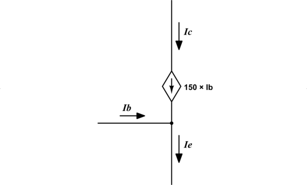
By removing everything that's not important for considerations of current, you're left with this:

simulate this circuit – Schematic created using CircuitLab
The presence or absence of the resistors and all the other elements is irrelevant to Kirchoff's Current Law (KCL), which when applied to the above is:
$$ I_E = I_B + I_C $$
\$I_E\$ and \$I_C\$ are only equal when \$I_B=0\$. Any non-zero \$I_B\$ will cause \$I_E \ne I_C\$, and there's no other way to interpret this system of currents.
In a twist of irony, if we treat the circuit in figure 3.54 exactly as drawn, with no closed loop around which \$I_B\$ can flow, then \$I_B=0\$. For a reason that has nothing to do with your question, it turns out that in this case you are accidentally correct: \$I_E = I_B + I_C = 0 + I_C = I_C\$.
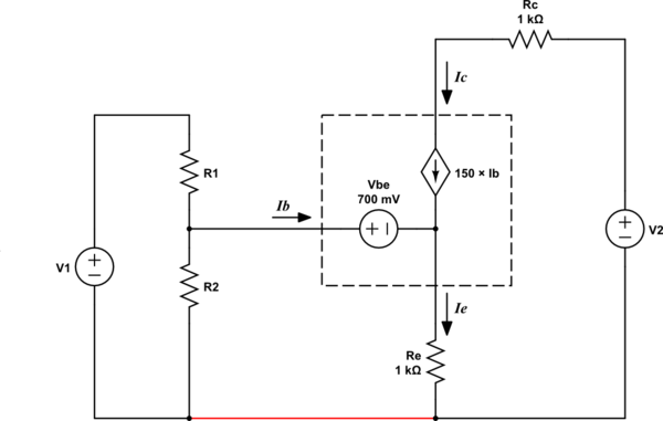
Just for completeness, to resolve the problem that the shown circuit cannot possibly produce any non-zero base current \$I_B\$, I believe what the author meant to draw (and should have drawn) would be this:

I added the red wire representing a point of equal potential between the two halves of the circuit, and providing a loop around which \$I_B\$ can flow, and be non-zero.
Everything in the dotted box represents (very naively) the transistor itself, with \$\beta=150\$, and \$V_{BE}=0.7V\$. KCL still applies:
$$ I_E = I_B + I_C $$
That is, total current entering the dotted box must equal total current leaving it. Otherwise there's an accumulation/depletion of charge inside the box, or a current leaking in/out somewhere that isn't being accounted for. Using the water analogy, it doesn't matter what that dotted box contains, as long as the plumbing inside doesn't have any leaks, and there's nothing in there to accumulate water (like a "ballooning" pipe), then for every litre of water entering the box (via any route) one litre must emerge somewhere else.
The full text of the question related to Fig. 3.54 is (Emphasis added):
- For the circuit of Fig. 3.54 (which is a model for the dc operation of a bipolar junction transistor biased in forward active region), \$I_B\$ is measured to be 100 μA. Determine \$I_C\$ and \$I_E\$
There's obviously a connection not shown (probably grounds missing from the left and right bottom nodes), but the point of the problem is to get you to apply KCL.
You can really ignore just about everything but the pink annotations and where the respective currents flow.